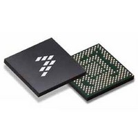
SC900841JVKR2 Freescale Semiconductor, SC900841JVKR2 Datasheet - Page 42

SC900841JVKR2
Manufacturer Part Number
SC900841JVKR2
Description
IC POWER MGT 338-MAPBGA
Manufacturer
Freescale Semiconductor
Specifications of SC900841JVKR2
Applications
PC's, PDA's
Operating Temperature
-40°C ~ 85°C
Mounting Type
Surface Mount
Package / Case
338-TBGA
Input Voltage
2.8 V to 4.4 V
Maximum Operating Temperature
+ 85 C
Minimum Operating Temperature
- 40 C
Lead Free Status / RoHS Status
Lead free / RoHS Compliant
Current - Supply
-
Voltage - Supply
-
Lead Free Status / Rohs Status
Lead free / RoHS Compliant
Available stocks
Company
Part Number
Manufacturer
Quantity
Price
Company:
Part Number:
SC900841JVKR2
Manufacturer:
Freescale Semiconductor
Quantity:
10 000
- Current page: 42 of 192
- Download datasheet (8Mb)
Table 7. COMMs Modules Interface Pin Functionality
COMMS MODULE INTERFACE
modules:
voltage rails that support the Advanced COMMs module(s):
VYMXGPS, VYMXPA, and VYMX3G.
hardware or software. If a software control is desired, the
enable input signal must always be active, and the internal
SPI register is used to turn on/off the output voltage. If
hardware control is desired, the internal SPI register must be
configured to turn on the voltage rail, and the ENABLE pin is
used to enable/disable the voltage rail.
42
900841
FUNCTIONAL DEVICE OPERATION
SYSTEM CONTROL INTERFACE
1. Basic COMMs: WiFi, Bluetooth (BT), and GPS. The
2. Advanced COMMs: WiMax and 3G options.
The 900841 supports the following communication
The 900841 provides a set of pins to enable/disable the
The Advanced COMMs rails can be controlled either by
VYMXGPSEN
VYMXPAEN
VYMX3GEN
Pin Name
basic COMMs subsystem is present on all Ultra-mobile
Platforms.
Enable Input signal for the VYMXGPS rail.
Only applicable when the VYMXGPS rail is
set to the 1.3 V option.
Enable Input signal for the VYMXPA rail. Only
applicable when the VYMXPA rail is set to the
4.2V option.
Enable Input signal for the VYMX3G rail
Figure 7. SPI Interface Timing Diagram (Processor Input capacitance is 3.0 pF)
Figure 6. SPI Write to PMIC Diagram (One address/Data Packet Shown)
Pin Functionality
rails. For a voltage rail to be active, both the SPI register
setting and the ENABLE pin must be active.
the pin is left open, the enable signal will be asserted low by
the internal pull-down, and the voltage rail will be inactive.
in
Advanced COMMs Serial Interface
through a simple serial interface, referred to as the “Mini-SPI”
in this document. This interface is used to control the output
voltage levels of the Advanced COMMs rails and has the
following characteristics:
• SPI maximum clock speed is 10 MHz
• SPI interface consists of 16-bit word
• MSB Bit 15 is sent first followed by MSB-1 and so forth.
• SPI configured with rising-edge clock where data is
• CS (Chip Select) indicates when the master starts SPI
Table 8. COMMs Modules Interface Pins vs. Control
Signal
OFF (Low)
OFF (Low)
ON (High)
ON (High)
Table 3
Table 8
Each enable pin includes an internal pull-down resistor. If
The enable signals follow the DC signaling specifications
The advanced COMMs module interfaces with the 900841
sampled on the rising edge of clock
data exchange. It is also used to reset the SPI slave so that
with a reference of 1.8 V (VPMIC).
shows the control logic of the Advanced COMMs
Registers
Register Setting
OFF
ON
OFF
ON
Analog Integrated Circuit Device Data
Freescale Semiconductor
Rail Output
OFF
OFF
OFF
ON
Related parts for SC900841JVKR2
Image
Part Number
Description
Manufacturer
Datasheet
Request
R
Part Number:
Description:
Ultra-mobile Platform Pmic
Manufacturer:
Freescale Semiconductor, Inc
Datasheet:

Part Number:
Description:
Sc900 Programmable Penta Uldo With Reset And I2c Interface
Manufacturer:
Semtech Corporation
Datasheet:
Part Number:
Description:
Manufacturer:
Freescale Semiconductor, Inc
Datasheet:
Part Number:
Description:
Manufacturer:
Freescale Semiconductor, Inc
Datasheet:
Part Number:
Description:
Manufacturer:
Freescale Semiconductor, Inc
Datasheet:
Part Number:
Description:
Manufacturer:
Freescale Semiconductor, Inc
Datasheet:
Part Number:
Description:
Manufacturer:
Freescale Semiconductor, Inc
Datasheet:
Part Number:
Description:
Manufacturer:
Freescale Semiconductor, Inc
Datasheet:
Part Number:
Description:
Manufacturer:
Freescale Semiconductor, Inc
Datasheet:
Part Number:
Description:
Manufacturer:
Freescale Semiconductor, Inc
Datasheet:
Part Number:
Description:
Manufacturer:
Freescale Semiconductor, Inc
Datasheet:
Part Number:
Description:
Manufacturer:
Freescale Semiconductor, Inc
Datasheet:
Part Number:
Description:
Manufacturer:
Freescale Semiconductor, Inc
Datasheet:
Part Number:
Description:
Manufacturer:
Freescale Semiconductor, Inc
Datasheet:
Part Number:
Description:
Manufacturer:
Freescale Semiconductor, Inc
Datasheet:


