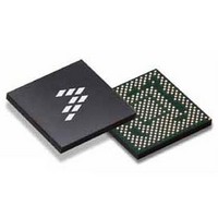
SC900841JVKR2 Freescale Semiconductor, SC900841JVKR2 Datasheet - Page 159

SC900841JVKR2
Manufacturer Part Number
SC900841JVKR2
Description
IC POWER MGT 338-MAPBGA
Manufacturer
Freescale Semiconductor
Specifications of SC900841JVKR2
Applications
PC's, PDA's
Operating Temperature
-40°C ~ 85°C
Mounting Type
Surface Mount
Package / Case
338-TBGA
Input Voltage
2.8 V to 4.4 V
Maximum Operating Temperature
+ 85 C
Minimum Operating Temperature
- 40 C
Lead Free Status / RoHS Status
Lead free / RoHS Compliant
Current - Supply
-
Voltage - Supply
-
Lead Free Status / Rohs Status
Lead free / RoHS Compliant
Available stocks
Company
Part Number
Manufacturer
Quantity
Price
Company:
Part Number:
SC900841JVKR2
Manufacturer:
Freescale Semiconductor
Quantity:
10 000
- Current page: 159 of 192
- Download datasheet (8Mb)
Table 97. Possible Reserved Channels Usage
occurs by asserting the following bits to 1. If the following bits
are 0, then these channels are reserved:
• VPWRCON for channel 22
• CHRGICON for channel 24
• LICON for channel 25
• BATDETVCON for channel 26
CONTROL
file, which stores the address of the analog input for
sampling. The 10-bit result is then stored in a separate
register file 10+1 bits wide and 32 entries deep.
setting the ADEN bit high in the ADCCNTL1 register. When
the register ADCCNTL1 ADSTRT bit is enabled, the PMIC
will cycle through the 3 + 5 bit selector addresses in registers
ADCADDRx. The high 3-bits control the touch screen bias
FETs, as described in
bits address the ADC selector to connect one of 32 channels
Table 98. ADC LSB Settings
Analog Integrated Circuit Device Data
Freescale Semiconductor
Notes
32.
#
0
1
2
3
4
5
6
7
8
9
Activating the prior channels to provide the signal specified
The ADC block consists of a 5-bit wide, 32-entry register
In order to operate the ADC, it has to be enabled first by
24
25
26
27
28
29
30
31
Equivalent to -3.0 to +3.0 A of current with a 100 mOhm sense resistor
SELECT[4:0]
00000
00001
00010
00011
00100
00101
00110
00111
01000
01001
Touch Screen
Backup Voltage (V
(V
ISNSBATP
Battery Pack Thermistor
VCC180 Current Sense
PMIC Die Temperature
Battery Voltage (V
VDDQ Current Sense
ADC INPUT SIGNAL
Charger Current
VCC Current Sense
VNN Current Sense
V33 Current Sense
(V
Battery Detect
Adaptor Voltage
Battery Current
BAT –
Reserved
Reserved
Reserved
Reserved
Reserved
– V
Interface. The lower 5-
V
ISNSBATN
ISNSBATN
COINCELL
BAT
)
)
)
)
6.0 A (-3.0 to 3.0 A)
SIGNAL RANGE
1.2 – 2.4 V
4.2 A
1.9 A
0.5 A
1.8 A
1.7 A
4.8 V
2.4 V
24 V
-300 – 300 mV
to the ADC. The result of the ADC conversion is stored into
the result registers (ADCSNSx), along with the input gain
setting (1 MSB). An address in the selector table of 0x1F
designates the stop location of the selection loop. At which
point the interrupt flag bit 0 (RND), which can be masked
through the MRND bit in the MADCINT register, is set in
register ADCINT, bit 1 of the INTERRUPT register (ADC) is
set, and the external PMICINT signal is asserted, if bit 1 of the
INTMASK register is clear. The ADC sleeps for 0 to 27 ms as
set by ADC register ADCCNTL1 through the ADSLP[2:0] bits
and then repeats the selector cycle. The new data overwrites
the old in the result registers. At most, all 32 result registers
will be filled within 15.625 ms (2048/32 = 1/64 Hz). The result
registers will not be read until the RND flag is set.
DEDICATED CHANNELS READING
LSBSEL bit in the FSLADCCNTL register. LSBSEL = 0 is the
default setting. See
Two different LSB value settings are possible by using the
0 – V
Reserved
Reserved
Reserved
Reserved
Reserved
0 – 3.6 V
CORE
(32)
(LSBSEL = 0)
LSB VALUE
23.4375 mV
4.1015 mA
1.8554 mA
0.4883 mA
1.7578 mA
1.6602 mA
4.6875 mV
5.8594 mA
2.3438 mV
Table 98
0.4244 K
Reserved
Reserved
Reserved
Reserved
Reserved
FUNCTIONAL DEVICE OPERATION
x2/3
x5/6
x4
for more information
(LSBSEL = 1)
ADC SUBSYSTEM
LSB VALUE
-1.2– +1.2 V
0 – 2.31 V
Reserved
Reserved
Reserved
Reserved
Reserved
0 – 2.4 V
10 mA
10 mA
10 mA
10 mA
10 mA
10 mV
10 mA
10 mV
10mV
1C
900841
159
Related parts for SC900841JVKR2
Image
Part Number
Description
Manufacturer
Datasheet
Request
R
Part Number:
Description:
Ultra-mobile Platform Pmic
Manufacturer:
Freescale Semiconductor, Inc
Datasheet:

Part Number:
Description:
Sc900 Programmable Penta Uldo With Reset And I2c Interface
Manufacturer:
Semtech Corporation
Datasheet:
Part Number:
Description:
Manufacturer:
Freescale Semiconductor, Inc
Datasheet:
Part Number:
Description:
Manufacturer:
Freescale Semiconductor, Inc
Datasheet:
Part Number:
Description:
Manufacturer:
Freescale Semiconductor, Inc
Datasheet:
Part Number:
Description:
Manufacturer:
Freescale Semiconductor, Inc
Datasheet:
Part Number:
Description:
Manufacturer:
Freescale Semiconductor, Inc
Datasheet:
Part Number:
Description:
Manufacturer:
Freescale Semiconductor, Inc
Datasheet:
Part Number:
Description:
Manufacturer:
Freescale Semiconductor, Inc
Datasheet:
Part Number:
Description:
Manufacturer:
Freescale Semiconductor, Inc
Datasheet:
Part Number:
Description:
Manufacturer:
Freescale Semiconductor, Inc
Datasheet:
Part Number:
Description:
Manufacturer:
Freescale Semiconductor, Inc
Datasheet:
Part Number:
Description:
Manufacturer:
Freescale Semiconductor, Inc
Datasheet:
Part Number:
Description:
Manufacturer:
Freescale Semiconductor, Inc
Datasheet:
Part Number:
Description:
Manufacturer:
Freescale Semiconductor, Inc
Datasheet:


