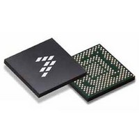
SC900841JVKR2 Freescale Semiconductor, SC900841JVKR2 Datasheet - Page 44

SC900841JVKR2
Manufacturer Part Number
SC900841JVKR2
Description
IC POWER MGT 338-MAPBGA
Manufacturer
Freescale Semiconductor
Specifications of SC900841JVKR2
Applications
PC's, PDA's
Operating Temperature
-40°C ~ 85°C
Mounting Type
Surface Mount
Package / Case
338-TBGA
Input Voltage
2.8 V to 4.4 V
Maximum Operating Temperature
+ 85 C
Minimum Operating Temperature
- 40 C
Lead Free Status / RoHS Status
Lead free / RoHS Compliant
Current - Supply
-
Voltage - Supply
-
Lead Free Status / Rohs Status
Lead free / RoHS Compliant
Available stocks
Company
Part Number
Manufacturer
Quantity
Price
Company:
Part Number:
SC900841JVKR2
Manufacturer:
Freescale Semiconductor
Quantity:
10 000
• When the 2nd level register is read, any 2nd level register
Table 10. Interrupt Registers Summary
44
900841
FUNCTIONAL DEVICE OPERATION
SYSTEM CONTROL INTERFACE
Notes
CHARGE
CHARGE
POWER
POWER
12.
13.
14.
15.
16.
17.
AUDIO
AUDIO
bits that were set at the point the SPI read strobe sweeps,
the register value into the SPI transmit shift register, that
bit will be cleared by the SPI self clear signal immediately
following the read strobe. This allows new interrupts to be
Block
GPIO
RTC
ADC
ADC
IRQ
IRQ
R
R
Because of the design of the clear on read logic, any interrupt event is allowed to happen at any time. If the interrupt event happens
close to when a read of the interrupt register happens, if the SPI read captures that interrupt bit as being set, then that bit will get cleared.
If the read does not capture the bit as being set, it will not be cleared. In this way no interrupt events are lost.
The 2nd level interrupts that get "Ored" together to set the 1st level interrupt bits can block other 2nd level interrupts from setting the 1st
level interrupt register. This is because if any of the 2nd level interrupts is high, the output of the OR will remain high, blocking the other
2nd level interrupt’s rising edge. This should not be a problem. because when the 2nd level register is read, the SCU will see all the bits
that are active when it is read. The software will decide which one to service first, just as it needs to do when more than one 1st level
interrupt bits are set when that register is read.
Masking has no affect on interrupt bits being set or cleared. Masking just prevents the interrupt event from asserting the interrupt pin. If
an interrupt bit is set, but is masked, the interrupt pin does not assert. If the mask bit is cleared while the bit is still set, the interrupt pin
will assert. Most interrupt registers have 1st and 2nd level mask bits. Both mask bits must be in the unmasked state to generate an
interrupt to the SCU.
Some 2nd level interrupt registers are level sensitive. If the level that sets these interrupts registers is active when the register is read,
it will clear during the active time of the clear on read signal and then reassert. This will reassert the 1st level interrupt bit.
The GPIO interrupts do not have interrupt masking bits, they have interrupt prevention bits. This is controlled by bits 5:4 of the GPIO
control register. See
Interrupts generated by external events are de-bounced. Therefore, the event needs to be stable throughout the de-bounce period
before an interrupt is generated. Nominal de-bounce periods for each event are documented in
nature of the de-bounce timer, the effective de-bounce time can vary slightly.
Address
0X197
0X198
0x1C
0xD0
0xD1
0x04
0x05
0x30
0x31
0x5F
0x60
0xE8
INTERRUP
VRFAULTI
MVRFAUL
MCHRGIN
MADCINT
CHRGINT
INTMASK
GPIOINT
Register
ADCINT
AUD24
AUD25
Name
RTCC
TINT
GPIOs
NT
T
T
for more details on using the GPIO as interrupt inputs.
R/W
R/W
R/W
R/W MUSBO
RW
RW
R
R
R
R
R
R
R
GPIINT7 GPIINT6 GPIINT5 GPIINT4 GPIINT3
USBOV
MEXT
RSVD
RSVD
RSVD
RSVD
RSVD
RSVD
IRQF
EXT
D7
VP
P
MDCLM
DCLMT BATDET USBDE
PF (=0)
MAUX
RSVD
RSVD
RSVD
RSVD
RSVD
RSVD
AUX
D6
T
MVRFAU
MBATDE
VRFAUL
RSVD
RSVD
RSVD
RSVD
RSVD
RSVD
D5
LT
AF
T
T
MUSBD
MGPIO
recorded without being lost. If a new unmasked 2nd level
interrupt event happens just after the read of the 2nd level
register, the PMICINT pin will assert if the 1st level bit is
not masked.
RSVD
RSVD
RSVD
RSVD
RSVD
RSVD
GPIO
D4
UF
ET
T
MCOMP
MHSDE
HSDET
COMP
MRTC
RSVD
RSVD
RSVD
RSVD
RSVD
RTC
D3
T
OVERFLO
MOVERFL
MVRFAIL
MHPDET
GPIINT2
MTEMP
VRFAIL
HPDET
MCHR
RSVD
TEMP
Analog Integrated Circuit Device Data
CHR
OW
D2
W
Table
11. Due to the asynchronous
MBATOVP
MPENDET
SWMPINT SWLPINT
MBATOC
MSWMPI
BATOCP
PENDET
BATOVP
GPIINT1
MADC
RSVD
ADC
Freescale Semiconductor
NT
D1
P
MSWLPIN
MPWRBT
PWRBTN
GPIINT0
MTHRM
MRND
THRM
RSVD
RSVD
RSVD
RND
D0
N
T
Initial
0xFA
0X00
0X0F
0x00
0x00
0x00
0x03
0x00
0x00
0x00
0x00
0x00


