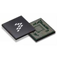
SC900841JVKR2 Freescale Semiconductor, SC900841JVKR2 Datasheet - Page 34

SC900841JVKR2
Manufacturer Part Number
SC900841JVKR2
Description
IC POWER MGT 338-MAPBGA
Manufacturer
Freescale Semiconductor
Specifications of SC900841JVKR2
Applications
PC's, PDA's
Operating Temperature
-40°C ~ 85°C
Mounting Type
Surface Mount
Package / Case
338-TBGA
Input Voltage
2.8 V to 4.4 V
Maximum Operating Temperature
+ 85 C
Minimum Operating Temperature
- 40 C
Lead Free Status / RoHS Status
Lead free / RoHS Compliant
Current - Supply
-
Voltage - Supply
-
Lead Free Status / Rohs Status
Lead free / RoHS Compliant
Available stocks
Company
Part Number
Manufacturer
Quantity
Price
Company:
Part Number:
SC900841JVKR2
Manufacturer:
Freescale Semiconductor
Quantity:
10 000
- Current page: 34 of 192
- Download datasheet (8Mb)
Table 5. SC900841 Pin Description
34
VOUTYMXGPS33
900841
FUNCTIONAL DESCRIPTION
GENERAL DESCRIPTION
VOUTPNL33
VCOREREF
Node Name
VOUTGP33
VCOREDIG
LDOREFP8
LDOREFP9
GNDCORE
VOUTVIB
PVIN3P3
PVINVIB
SDIOGT
FBSDIO
VCORE
I2SVCC
BCL1
BCL2
FS1
RX1
TX1
FS2
RX2
TX2
LOPWRGND
MDPWR
MDPWR
MDPWR
LOPWR
LOPWR
LOPWR
LOPWR
LOPWR
LOPWR
LOPWR
LOPWR
LOPWR
LOPWR
SGNL
SGNL
SGNL
SGNL
SGNL
SGNL
SGNL
SGNL
SGNL
Type
I/O
I/O
I/O
I/O
I/O
O
O
-
-
-
-
-
-
-
-
-
-
-
-
-
-
-
I
I
Rating
VSDIO - 3.3 V/215 mA Switch OR 1.8 V/215 mA LDO
4.8 V
3.6 V
3.6 V
3.6 V
3.6 V
3.6 V
3.6 V
3.6 V
3.6 V
1.5 V
3.6 V
3.6 V
3.6 V
3.6 V
3.6 V
3.6 V
3.6 V
3.6 V
3.6 V
3.6 V
3.6 V
3.6 V
-
VYMXGPS33 - 3.3 V/60 mA Switch
Balls
# of
VPNL33 - 3.3 V/100 mA Switch
1
1
1
1
1
1
1
1
1
1
1
1
1
1
1
1
1
1
1
1
1
1
1
VGP33 - 3.3 V/60 mA Switch
VVIB - xV/200 mA LDO
Internal Supplies
BGA Location
Audio Bus
AG13
AH10
AB12
AC13
AJ13
AG9
AH8
C13
G13
H14
H28
AJ9
B14
L25
K28
L27
L23
K22
K26
J13
J29
J27
B6
Power Supply Input for VVIB and Reference Generation.
This must always be connected to VPWR.
VVIB Output Voltage Node
Power Supply Input, shared by VPNL33, VGP33,
VYMXGPS33 and VSDIO
VPNL33 Output Voltage Node
VPG33 Output Voltage Node
VYMXGPS33 Output Voltage Node
Gate Driver Output for VSDIO pass FET
Internal Supply Output Voltage Node
Internal Supply Output Voltage Node
Internal BandGap Supply Output Voltage Node
Internal Divided Down BandGap Supply Output Voltage
Node dedicated for LDOs
Internal Divided Down BandGap Supply Output Voltage
Node dedicated for LDOs
Ground for Internal Supplies
Supply Voltage to the I2S Bus
Bit clock for audio bus 1. Input in slave mode, output in
master mode
Frame synchronization clock for audio bus 1. Input in slave
mode, output in master mode.
Receive Data for audio bus 1
Transmit data for audio bus 1
Bit clock for audio bus 2. Input in slave mode, output in
master mode
Frame synchronization clock for audio bus 2. Input in slave
mode, output in master mode.
Receive Data for audio bus 2
Transmit data for audio bus 2
Feedback node when VSDIO is in Switch mode; Output
voltage node when VSDIO is in LDO mode.
Analog Integrated Circuit Device Data
Pin Description
Freescale Semiconductor
Related parts for SC900841JVKR2
Image
Part Number
Description
Manufacturer
Datasheet
Request
R
Part Number:
Description:
Ultra-mobile Platform Pmic
Manufacturer:
Freescale Semiconductor, Inc
Datasheet:

Part Number:
Description:
Sc900 Programmable Penta Uldo With Reset And I2c Interface
Manufacturer:
Semtech Corporation
Datasheet:
Part Number:
Description:
Manufacturer:
Freescale Semiconductor, Inc
Datasheet:
Part Number:
Description:
Manufacturer:
Freescale Semiconductor, Inc
Datasheet:
Part Number:
Description:
Manufacturer:
Freescale Semiconductor, Inc
Datasheet:
Part Number:
Description:
Manufacturer:
Freescale Semiconductor, Inc
Datasheet:
Part Number:
Description:
Manufacturer:
Freescale Semiconductor, Inc
Datasheet:
Part Number:
Description:
Manufacturer:
Freescale Semiconductor, Inc
Datasheet:
Part Number:
Description:
Manufacturer:
Freescale Semiconductor, Inc
Datasheet:
Part Number:
Description:
Manufacturer:
Freescale Semiconductor, Inc
Datasheet:
Part Number:
Description:
Manufacturer:
Freescale Semiconductor, Inc
Datasheet:
Part Number:
Description:
Manufacturer:
Freescale Semiconductor, Inc
Datasheet:
Part Number:
Description:
Manufacturer:
Freescale Semiconductor, Inc
Datasheet:
Part Number:
Description:
Manufacturer:
Freescale Semiconductor, Inc
Datasheet:
Part Number:
Description:
Manufacturer:
Freescale Semiconductor, Inc
Datasheet:


