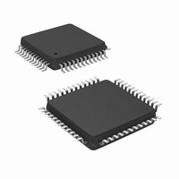
NUC100LC1BN Nuvoton Technology Corporation of America, NUC100LC1BN Datasheet - Page 347

NUC100LC1BN
Manufacturer Part Number
NUC100LC1BN
Description
IC MCU 32BIT 32KB FLASH 48LQFP
Manufacturer
Nuvoton Technology Corporation of America
Series
NuMicro™r
Specifications of NUC100LC1BN
Core Processor
ARM Cortex-M0
Core Size
32-Bit
Speed
50MHz
Connectivity
I²C, IrDA, SPI, UART/USART
Peripherals
Brown-out Detect/Reset, DMA, I²S, LVD, POR, PS2, PWM, WDT
Number Of I /o
35
Program Memory Size
32KB (32K x 8)
Program Memory Type
FLASH
Ram Size
4K x 8
Voltage - Supply (vcc/vdd)
2.5 V ~ 5.5 V
Data Converters
A/D 8x12b
Oscillator Type
Internal
Operating Temperature
-40°C ~ 85°C
Package / Case
48-LQFP
Lead Free Status / RoHS Status
Lead free / RoHS Compliant
Eeprom Size
-
Available stocks
Company
Part Number
Manufacturer
Quantity
Price
Company:
Part Number:
NUC100LC1BN
Manufacturer:
NuvoTon
Quantity:
1 600
Company:
Part Number:
NUC100LC1BN
Manufacturer:
Nuvoton Technology Corporation of America
Quantity:
10 000
Part Number:
NUC100LC1BN
Manufacturer:
NUVOTON
Quantity:
20 000
- NUC100LC1BN PDF datasheet
- NUC100LC1BN PDF datasheet #2
- NUC100LC1BN PDF datasheet #3
- NUC100LC1BN_PRODUCT_CHANGE PDF datasheet #4
- Current page: 347 of 600
- Download datasheet (6Mb)
Word Suspend
These four bits field of SP_CYCLE (SPI_CNTRL[15:12]) provide a configurable suspend interval
2 ~ 17 serial clock periods between two successive transaction words in master mode. The
suspend interval is from the last falling clock edge of the preceding transaction word to the first
rising clock edge of the following transaction word if CLKP = 0. If CLKP = 1, the interval is from
the rising clock edge of the preceding transaction word to the falling clock edge of the following
transaction word. The default value of SP_CYCLE is 0x0 (2 serial clock cycles), but set these bits
field has no any effects on data transaction process if TX_NUM = 0x00.
Byte Reorder
When the transfer is set as MSB first (LSB = 0) and the REORDER is enabled, the data stored in
the TX buffer and RX buffer will be rearranged in the order as [BYTE0, BYTE1, BYTE2, BYTE3]
in TX_BIT_LEN = 32 bits mode, and the sequence of transmitted/received data will be BYTE0,
BYTE1, BYTE2, and then BYTE3. If the TX_BIT_LEN is set as 24-bits mode, the data in TX
buffer and RX buffer will be rearranged as [unknown byte, BYTE0, BYTE1, BYTE2] and the
BYTE0, BYTE1, and BYTE2 will be transmitted/received data step by step in MSB first. The rule
of 16-bits mode is the same as above.
Byte3
MSB first
SPI_TX0/SPI_RX0
Byte2
NuMicro™ NUC100 Series Technical Reference Manual
Byte1
Byte0
Figure 5-55 Byte Reorder
& REORDER = 2'b10/2'b01
LSB = 0 (MSB first)
- 347 -
Publication Release Date: Oct 22, 2010
Byte0 Byte1 Byte2
nn
nn
MSB first
TX_BIT_LEN = 32 bits
TX_BIT_LEN = 24 bits
TX_BIT_LEN = 16 bits
TX/RX Buffer
Byte0
nn
MSB first
nn = unknown byte
Byte1
Byte0
Revision V1.06
MSB first
Byte3
Byte2
Byte1
Related parts for NUC100LC1BN
Image
Part Number
Description
Manufacturer
Datasheet
Request
R

Part Number:
Description:
Manufacturer:
Nuvoton Technology Corporation of America
Datasheet:

Part Number:
Description:
Manufacturer:
Nuvoton Technology Corporation of America
Datasheet:

Part Number:
Description:
Manufacturer:
Nuvoton Technology Corporation of America
Datasheet:

Part Number:
Description:
Manufacturer:
Nuvoton Technology Corporation of America
Datasheet:

Part Number:
Description:
Manufacturer:
Nuvoton Technology Corporation of America
Datasheet:

Part Number:
Description:
Manufacturer:
Nuvoton Technology Corporation of America
Datasheet:

Part Number:
Description:
Manufacturer:
Nuvoton Technology Corporation of America
Datasheet:


