NUC100LC1BN Nuvoton Technology Corporation of America, NUC100LC1BN Datasheet - Page 212
NUC100LC1BN
Manufacturer Part Number
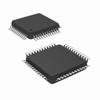
NUC100LC1BN
Description
IC MCU 32BIT 32KB FLASH 48LQFP
Manufacturer
Nuvoton Technology Corporation of America
Series
NuMicro™r
Specifications of NUC100LC1BN
Core Processor
ARM Cortex-M0
Core Size
32-Bit
Speed
50MHz
Connectivity
I²C, IrDA, SPI, UART/USART
Peripherals
Brown-out Detect/Reset, DMA, I²S, LVD, POR, PS2, PWM, WDT
Number Of I /o
35
Program Memory Size
32KB (32K x 8)
Program Memory Type
FLASH
Ram Size
4K x 8
Voltage - Supply (vcc/vdd)
2.5 V ~ 5.5 V
Data Converters
A/D 8x12b
Oscillator Type
Internal
Operating Temperature
-40°C ~ 85°C
Package / Case
48-LQFP
Lead Free Status / RoHS Status
Lead free / RoHS Compliant
Eeprom Size
-
Available stocks
Company
Part Number
Manufacturer
Quantity
Price
Company:

Part Number:
NUC100LC1BN
Manufacturer:
NuvoTon
Quantity:
1 600
Company:
Part Number:
NUC100LC1BN
Manufacturer:
Nuvoton Technology Corporation of America
Quantity:
10 000
Part Number:
NUC100LC1BN
Manufacturer:
NUVOTON
Quantity:
20 000


PLL Control Register (PLLCON)
The PLL reference clock input is from the external 4~24 MHz crystal clock input or from the
internal 22.1184 MHz oscillator. These registers are use to control the PLL output frequency and
PLL operating mode
Register
PLLCON
Bits
[31:20]
[19]
[18]
[17]
[16]
[15:14]
[13:9]
[8:0]
31
23
15
7
OUT_DV
NuMicro™ NUC100 Series Technical Reference Manual
Offset
CLK_BA+0x20
Descriptions
Reserved
PLL_SRC
OE
BP
PD
OUT_DV
IN_DV
FB_DV
30
22
14
6
Reserved
R/W
R/W
Reserved
PLL Source Clock Select
1 = PLL source clock from internal 22.1184 MHz oscillator
0 = PLL source clock from external 4~24 MHz crystal
PLL OE (FOUT enable) pin Control
0 = PLL FOUT enable
1 = PLL FOUT is fixed low
PLL Bypass Control
0 = PLL is in normal mode (default)
1 = PLL clock output is same as clock input (XTALin)
Power Down Mode
If set the PWR_DOWN_EN bit to 1 in PWRCON register, the PLL will enter power
down mode too.
0 = PLL is in normal mode
1 = PLL is in power-down mode (default)
PLL Output Divider Control Pins
Refer to the formulas below the table.
PLL Input Divider Control Pins
Refer to the formulas below the table.
PLL Feedback Divider Control Pins
Refer to the formulas below the table.
29
21
13
5
Description
PLL Control Register
28
20
12
4
- 212 -
Reserved
FB_DV
PLL_SRC
IN_DV
27
19
11
3
Publication Release Date: Dec. 22, 2010
OE
26
18
10
2
BP
25
17
9
1
Revision V1.06
Reset Value
0x0005_C22E
FB_DV
PD
24
16
8
0
Related parts for NUC100LC1BN
Image
Part Number
Description
Manufacturer
Datasheet
Request
R

Part Number:
Description:
Manufacturer:
Nuvoton Technology Corporation of America
Datasheet:
Part Number:
Description:
Manufacturer:
Nuvoton Technology Corporation of America
Datasheet:
Part Number:
Description:
Manufacturer:
Nuvoton Technology Corporation of America
Datasheet:
Part Number:
Description:
Manufacturer:
Nuvoton Technology Corporation of America
Datasheet:
Part Number:
Description:
Manufacturer:
Nuvoton Technology Corporation of America
Datasheet:
Part Number:
Description:
Manufacturer:
Nuvoton Technology Corporation of America
Datasheet:
Part Number:
Description:
Manufacturer:
Nuvoton Technology Corporation of America
Datasheet: