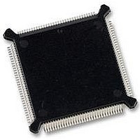
MC68331CEH20 Freescale Semiconductor, MC68331CEH20 Datasheet - Page 84

MC68331CEH20
Manufacturer Part Number
MC68331CEH20
Description
IC MCU 32BIT 20MHZ 132-PQFP
Manufacturer
Freescale Semiconductor
Series
M683xxr
Specifications of MC68331CEH20
Core Processor
CPU32
Core Size
32-Bit
Speed
20MHz
Connectivity
EBI/EMI, SCI, SPI, UART/USART
Peripherals
POR, PWM, WDT
Number Of I /o
18
Program Memory Type
ROMless
Voltage - Supply (vcc/vdd)
4.5 V ~ 5.5 V
Oscillator Type
Internal
Operating Temperature
-40°C ~ 85°C
Package / Case
132-QFP
Controller Family/series
68K
No. Of I/o's
18
Cpu Speed
20MHz
No. Of Timers
1
Embedded Interface Type
QSPI, SCI, UART
No. Of Pwm Channels
2
Digital Ic Case Style
PQFP
Rohs Compliant
Yes
Processor Series
M683xx
Core
CPU32
Data Bus Width
32 bit
Data Ram Size
80 B
Interface Type
QSPI, SCI, UART
Maximum Clock Frequency
20 MHz
Number Of Programmable I/os
18
Number Of Timers
1
Maximum Operating Temperature
+ 85 C
Mounting Style
SMD/SMT
Minimum Operating Temperature
- 40 C
Cpu Family
68K/M683xx
Device Core
ColdFire
Device Core Size
32b
Frequency (max)
20MHz
Program Memory Size
Not Required
Total Internal Ram Size
80Byte
# I/os (max)
18
Number Of Timers - General Purpose
1
Instruction Set Architecture
RISC
Operating Temp Range
-40C to 85C
Operating Temperature Classification
Industrial
Mounting
Surface Mount
Pin Count
132
Package Type
PQFP
Lead Free Status / RoHS Status
Lead free / RoHS Compliant
Eeprom Size
-
Ram Size
-
Program Memory Size
-
Data Converters
-
Lead Free Status / Rohs Status
Details
Available stocks
Company
Part Number
Manufacturer
Quantity
Price
Company:
Part Number:
MC68331CEH20
Manufacturer:
Freescale Semiconductor
Quantity:
10 000
Part Number:
MC68331CEH20
Manufacturer:
FREESCLA
Quantity:
20 000
4
4.6.5.2 Reset States of Pins Assigned to Other MCU Modules
4.6.6 Reset Timing
4-42
As a rule, module pins that are assigned to general-purpose I/O ports go to active high-
impedance state following reset. Other pin states are determined by individual module
control register settings. Refer to sections concerning modules for details. However,
during power-up reset, module port pins may be in an indeterminate state for a short
period. Refer to 4.6.7 Power-On Reset for more information.
The RESET input must be asserted for a specified minimum period for reset to occur.
External RESET assertion can be delayed internally for a period equal to the longest
bus cycle time (or the bus monitor time-out period) in order to protect write cycles from
being aborted by reset. While RESET is asserted, SIM pins are either in an inactive,
high impedance state or are driven to their inactive states.
When an external device asserts RESET for the proper period, reset control logic
clocks the signal into an internal latch. The control logic drives the RESET pin low for
an additional 512 CLKOUT cycles after it detects that the RESET signal is no longer
being externally driven, to guarantee this length of reset to the entire system.
CS[9:6]/ADDR[22:19]/PC[6:3]
IRQ[7:1]/PF[7:1]
SIZ[1:0]/PE[7:6]
CS10/ADDR23
CS5/FC2/PC2
CS3/FC0/PC0
MODCLK/PF0
DSACK0/PE0
DSACK1/PE1
CSE/BGACK
ADDR[18:0]
DATA[15:0]
Mnemonic
AVEC/PE2
CSBOOT
CLKOUT
FC1/PC1
CSM/BG
CS0/BR
AS/PE5
DS/PE4
RESET
BERR
HALT
RMC
R/W
TSC
Freescale Semiconductor, Inc.
For More Information On This Product,
Table 4-18 SIM Pin Reset States
SYSTEM INTEGRATION MODULE
High-Z Output
High-Z Output
Mode Select
Mode Select
Mode Select
State While
Asserted
Disabled
Disabled
Disabled
Disabled
Disabled
Disabled
Disabled
Disabled
Asserted
Disabled
Disabled
Go to: www.freescale.com
RESET
Output
1
1
1
1
1
1
1
1
1
ADDR[18:0]
DATA[15:0]
MODCLK
Function
CSBOOT
CLKOUT
DSACK0
DSACK1
IRQ[7:1]
SIZ[1:0]
CS[9:6]
RESET
BERR
AVEC
CS10
HALT
CSM
RMC
CSE
CS0
CS5
CS3
R/W
TSC
FC1
Pin
DS
AS
Pin State After RESET Released
Pin State
Unknown
Unknown
Output
Output
Output
Output
Output
Input
Input
Input
Input
Input
Input
Input
Input
Input
Input
1
1
1
1
1
0
1
1
1
ADDR[22:19]
ADDR[18:0]
DATA[15:0]
Function
CSBOOT
CLKOUT
ADDR23
BGACK
RESET
PF[7:1]
PE[7:6]
BERR
HALT
TSC
PE5
PE2
PE4
PE0
PE1
FC2
FC1
FC0
PF0
R/W
PE3
Pin
BG
BR
USER’S MANUAL
Pin State
Unknown
Unknown
Unknown
Unknown
Unknown
Unknown
Output
Output
Input
Input
Input
Input
Input
Input
Input
Input
Input
Input
Input
Input
Input
Input
Input
Input
MC68331
1
0


