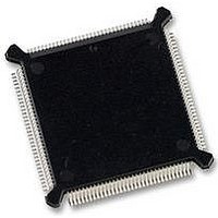
MC68331CEH20 Freescale Semiconductor, MC68331CEH20 Datasheet - Page 160

MC68331CEH20
Manufacturer Part Number
MC68331CEH20
Description
IC MCU 32BIT 20MHZ 132-PQFP
Manufacturer
Freescale Semiconductor
Series
M683xxr
Specifications of MC68331CEH20
Core Processor
CPU32
Core Size
32-Bit
Speed
20MHz
Connectivity
EBI/EMI, SCI, SPI, UART/USART
Peripherals
POR, PWM, WDT
Number Of I /o
18
Program Memory Type
ROMless
Voltage - Supply (vcc/vdd)
4.5 V ~ 5.5 V
Oscillator Type
Internal
Operating Temperature
-40°C ~ 85°C
Package / Case
132-QFP
Controller Family/series
68K
No. Of I/o's
18
Cpu Speed
20MHz
No. Of Timers
1
Embedded Interface Type
QSPI, SCI, UART
No. Of Pwm Channels
2
Digital Ic Case Style
PQFP
Rohs Compliant
Yes
Processor Series
M683xx
Core
CPU32
Data Bus Width
32 bit
Data Ram Size
80 B
Interface Type
QSPI, SCI, UART
Maximum Clock Frequency
20 MHz
Number Of Programmable I/os
18
Number Of Timers
1
Maximum Operating Temperature
+ 85 C
Mounting Style
SMD/SMT
Minimum Operating Temperature
- 40 C
Cpu Family
68K/M683xx
Device Core
ColdFire
Device Core Size
32b
Frequency (max)
20MHz
Program Memory Size
Not Required
Total Internal Ram Size
80Byte
# I/os (max)
18
Number Of Timers - General Purpose
1
Instruction Set Architecture
RISC
Operating Temp Range
-40C to 85C
Operating Temperature Classification
Industrial
Mounting
Surface Mount
Pin Count
132
Package Type
PQFP
Lead Free Status / RoHS Status
Lead free / RoHS Compliant
Eeprom Size
-
Ram Size
-
Program Memory Size
-
Data Converters
-
Lead Free Status / Rohs Status
Details
Available stocks
Company
Part Number
Manufacturer
Quantity
Price
Company:
Part Number:
MC68331CEH20
Manufacturer:
Freescale Semiconductor
Quantity:
10 000
Part Number:
MC68331CEH20
Manufacturer:
FREESCLA
Quantity:
20 000
7
7.2 GPT Registers and Address Map
7-2
The GPT programming model consists of a configuration register (GPTMCR), parallel
I/O registers (DDRGP, PORTGP), capture/compare registers (TCNT, TCTL1, TCTL2,
TIC[1:3], TOC[1:4], TI4/O5, CFORC), pulse accumulator registers (PACNT, PACTL),
pulse-width modulation registers (PWMA, PWMB, PWMC, PWMCNT, PWMBUFA,
PWMBUFB), status registers (TFLG1, TFLG2) and interrupt control registers (TMSK1,
TMSK2). Functions of the module configuration register are discussed in 7.3 Special
Modes of Operation and 7.4 Polled and Interrupt-Driven Operation. Other register
functions are discussed in the appropriate sections.
All registers can be accessed using byte or word operations. Certain capture/compare
registers and pulse-width modulation registers must be accessed by word operations
to ensure coherency. If byte accesses are used to read a register such as the timer
counter register (TCNT), there is a possibility that data in the byte not being accessed
will change while the other byte is read. Both bytes must be accessed at the same
time.
The modmap (MM) bit in the system integration module configuration register (SIM-
CR) defines the most significant bit (ADDR23) of the IMB address for each register in
the MCU.
Refer to APPENDIX D REGISTER SUMMARY for a GPT address map and register
bit/field descriptions. SECTION 4 SYSTEM INTEGRATION MODULE contains more
information about how the state of MM affects the system.
IC1/PGP0
IC3/PGP2
IC2/PGP1
Freescale Semiconductor, Inc.
For More Information On This Product,
Figure 7-1 GPT Block Diagram
GENERAL-PURPOSE TIMER
Go to: www.freescale.com
CAPTURE/COMPARE UNIT
PULSE ACCUMULATOR
BUS INTERFACE
PRESCALER
PWM UNIT
IMB
OC1/PGP3
OC2/OC1/PGP4
OC3/OC1/PGP5
OC4/OC1/PGP6
IC4/OC5/OC1/PGP7
PAI
PCLK
PWMA
PWMB
GPT BLOCK
USER’S MANUAL
MC68331


