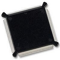
MC68331CEH20 Freescale Semiconductor, MC68331CEH20 Datasheet - Page 171

MC68331CEH20
Manufacturer Part Number
MC68331CEH20
Description
IC MCU 32BIT 20MHZ 132-PQFP
Manufacturer
Freescale Semiconductor
Series
M683xxr
Specifications of MC68331CEH20
Core Processor
CPU32
Core Size
32-Bit
Speed
20MHz
Connectivity
EBI/EMI, SCI, SPI, UART/USART
Peripherals
POR, PWM, WDT
Number Of I /o
18
Program Memory Type
ROMless
Voltage - Supply (vcc/vdd)
4.5 V ~ 5.5 V
Oscillator Type
Internal
Operating Temperature
-40°C ~ 85°C
Package / Case
132-QFP
Controller Family/series
68K
No. Of I/o's
18
Cpu Speed
20MHz
No. Of Timers
1
Embedded Interface Type
QSPI, SCI, UART
No. Of Pwm Channels
2
Digital Ic Case Style
PQFP
Rohs Compliant
Yes
Processor Series
M683xx
Core
CPU32
Data Bus Width
32 bit
Data Ram Size
80 B
Interface Type
QSPI, SCI, UART
Maximum Clock Frequency
20 MHz
Number Of Programmable I/os
18
Number Of Timers
1
Maximum Operating Temperature
+ 85 C
Mounting Style
SMD/SMT
Minimum Operating Temperature
- 40 C
Cpu Family
68K/M683xx
Device Core
ColdFire
Device Core Size
32b
Frequency (max)
20MHz
Program Memory Size
Not Required
Total Internal Ram Size
80Byte
# I/os (max)
18
Number Of Timers - General Purpose
1
Instruction Set Architecture
RISC
Operating Temp Range
-40C to 85C
Operating Temperature Classification
Industrial
Mounting
Surface Mount
Pin Count
132
Package Type
PQFP
Lead Free Status / RoHS Status
Lead free / RoHS Compliant
Eeprom Size
-
Ram Size
-
Program Memory Size
-
Data Converters
-
Lead Free Status / Rohs Status
Details
Available stocks
Company
Part Number
Manufacturer
Quantity
Price
Company:
Part Number:
MC68331CEH20
Manufacturer:
Freescale Semiconductor
Quantity:
10 000
Part Number:
MC68331CEH20
Manufacturer:
FREESCLA
Quantity:
20 000
7.8.3.1 Output Compare 1
7.8.3.2 Forced Output Compare
7.9 Input Capture 4/Output Compare 5
MC68331
USER’S MANUAL
When the programmed content of an output compare register matches the value in
TCNT, an output compare status flag (OCxF) bit in TFLG1 is set. If the appropriate in-
terrupt enable bit (OCxI) in TMSK1 is set, an interrupt request is made when a match
occurs. Refer to 7.4.2 GPT Interrupts for more information.
Operation of output compare 1 differs from that of the other output compare functions.
OC1 control logic can be programmed to make state changes on other OC pins when
an OC1 match occurs. Control bits in the timer compare force register (CFORC) allow
for early forced compares.
Output compare 1 can affect any or all of OC[1:5] when an output match occurs. In
addition to allowing generation of multiple control signals from a single comparison op-
eration, this function makes it possible for two or more output compare functions to
control the state of a single OC pin. Output pulses as short as one timer count can be
generated in this way.
The OC1 action mask register (OC1M) and the OC1 action data register (OC1D) con-
trol OC1 function. Setting a bit in OC1M selects a corresponding bit in the GPT parallel
data port. Bits in OC1D determine whether selected bits are to be set or cleared when
an OC1 match occurs. Pins must be configured as outputs in order for the data in the
register to be driven out on the corresponding pin. If an OC1 match and another output
match occur at the same time and both attempt to alter the same pin, the OC1 function
controls the state of the pin.
Timer compare force register (CFORC) is used to make forced compares. The action
taken as a result of a forced compare is the same as when an output compare match
occurs, except that status flags are not set. Forced channels take programmed actions
immediately after the write to CFORC.
The CFORC register is implemented as the upper byte of a 16-bit register which also
contains the PWM control register C (PWMC). It can be accessed as eight bits or a
word access can be used. Reads of force compare bits (FOC) have no meaning and
always return zeros. These bits are self-negating.
The IC4/OC5 pin can be used for input capture, output compare, or general-purpose
I/O. A function enable bit (I4/O5) in the pulse accumulator control register (PACTL)
configures the pin for input capture (IC4) or output compare function (OC5). Both bits
are cleared during reset, configuring the pin as an input, but also enabling the OC5
function. IC4/OC5 I/O functions are controlled by the I4/O5 bit in the port GP data di-
rection register (DDRGP).
The 16-bit register (TI4/O5) used with the IC4/OC5 function acts as an input capture
register or as an output compare register depending on which function is selected.
When used as the input capture 4 register, it cannot be written except in test or freeze
mode.
Freescale Semiconductor, Inc.
For More Information On This Product,
GENERAL-PURPOSE TIMER
Go to: www.freescale.com
7-13
7


