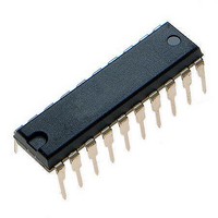
MCHC705JJ7CPE Freescale Semiconductor, MCHC705JJ7CPE Datasheet - Page 98

MCHC705JJ7CPE
Manufacturer Part Number
MCHC705JJ7CPE
Description
IC MCU 8BIT 224 BYTES RAM 20PDIP
Manufacturer
Freescale Semiconductor
Series
HC05r
Datasheet
1.MC705JJ7CDWE.pdf
(164 pages)
Specifications of MCHC705JJ7CPE
Core Processor
HC05
Core Size
8-Bit
Speed
2.1MHz
Connectivity
SIO
Peripherals
POR, Temp Sensor, WDT
Number Of I /o
14
Program Memory Size
6KB (6K x 8)
Program Memory Type
OTP
Ram Size
224 x 8
Voltage - Supply (vcc/vdd)
2.7 V ~ 5.5 V
Data Converters
A/D 4x12b
Oscillator Type
Internal
Operating Temperature
-40°C ~ 85°C
Package / Case
20-DIP (0.300", 7.62mm)
Processor Series
HC705JJ
Core
HC05
Data Bus Width
8 bit
Data Ram Size
224 B
Interface Type
SIOP
Maximum Clock Frequency
2.1 MHz
Number Of Programmable I/os
14
Number Of Timers
2
Maximum Operating Temperature
+ 85 C
Mounting Style
Through Hole
Minimum Operating Temperature
- 40 C
On-chip Adc
12 bit, 4 Channel
Package
20PDIP
Family Name
HC05
Maximum Speed
2.1 MHz
Operating Supply Voltage
3.3|5 V
Lead Free Status / RoHS Status
Lead free / RoHS Compliant
Eeprom Size
-
Lead Free Status / Rohs Status
Details
Simple Synchronous Serial Interface
SPE — Serial Peripheral Enable Bit
LSBF — Least Significant Bit First Bit
MSTR — Master Mode Select Bit
SPIR — Serial Peripheral Interrupt Reset Bit
CPHA — Clock Phase Bit
SPR0:1 — Serial Peripheral Clock Rate Select Bits
98
The SPE bit switches the port B interface such that SDO/PB5 is the serial data output, SDI/PB6 is the
serial data input, and SCK/PB7 is a serial clock input in the slave mode or a serial clock output in the
master mode. The port B DDR and data registers can be manipulated as usual, but these actions will
not affect the transmitted or received data. The SPE bit is readable and writable at any time, but
clearing the SPE bit while a transmission is in progress will 1) abort the transmission, 2) reset the serial
bit counter, and 3) convert port B to a general-purpose I/O port. Reset clears the SPE bit.
The LSBF bit controls the format of the transmitted and received data to be transferred LSB or MSB
first. Reset clears this bit.
The MSTR bit configures the serial I/O port for master mode. A transfer is initiated by writing to the
SDR. Also, the SCK pin becomes an output providing a synchronous data clock dependent upon the
divider of the oscillator frequency selected by the SPR0:1 bits. When the device is in master mode, the
SDO and SDI pins do not change function. These pins behave exactly the same in both the master
and slave modes. The MSTR bit is readable and writable at any time regardless of the state of the SPE
bit. Clearing the MSTR bit will abort any transfers that may have been in progress. Reset clears the
MSTR bit, placing the SIOP subsystem in slave mode.
The SPIR bit is a write-only control to reset the SPIF flag bit in the SSR. Reading the SPIR bit will return
a logic 0.
The CPHA bit controls the clock timing and phase in the SIOP. Data is changed on the falling edge of
SCK and data is captured (read) on the rising edge of SCK. This bit is cleared by reset.
The SPR0 and SPR1 bits select one of four clock rates given in
PB7/SCK pin when the device is configured with the SIOP as a master (MSTR = 1). The fastest rate
is when both SPR0 and SPR1 are set. Both the SPR0 and SPR1 bits are cleared by reset, which
places the SIOP clock selection at the slowest rate.
1 = Serial peripheral enabled (port B I/O disabled)
0 = Serial peripheral disabled (port B I/O enabled)
1 = LSB transferred first
0 = MSB transferred first
1 = SIOP set up as master, SCK is an output
0 = SIOP set up as slave, SCK is an input
1 = Reset the SPIF flag bit
0 = No effect
1 = SCK is idle low
0 = SCK is idle high
to determine the source of the interrupt and will vector to the reset vector
as a default.
MC68HC705JJ7 • MC68HC705JP7 Advance Information Data Sheet, Rev. 4.1
Table 9-1
to be supplied on the
Freescale Semiconductor


