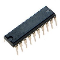
MCHC705JJ7CPE Freescale Semiconductor, MCHC705JJ7CPE Datasheet - Page 111

MCHC705JJ7CPE
Manufacturer Part Number
MCHC705JJ7CPE
Description
IC MCU 8BIT 224 BYTES RAM 20PDIP
Manufacturer
Freescale Semiconductor
Series
HC05r
Datasheet
1.MC705JJ7CDWE.pdf
(164 pages)
Specifications of MCHC705JJ7CPE
Core Processor
HC05
Core Size
8-Bit
Speed
2.1MHz
Connectivity
SIO
Peripherals
POR, Temp Sensor, WDT
Number Of I /o
14
Program Memory Size
6KB (6K x 8)
Program Memory Type
OTP
Ram Size
224 x 8
Voltage - Supply (vcc/vdd)
2.7 V ~ 5.5 V
Data Converters
A/D 4x12b
Oscillator Type
Internal
Operating Temperature
-40°C ~ 85°C
Package / Case
20-DIP (0.300", 7.62mm)
Processor Series
HC705JJ
Core
HC05
Data Bus Width
8 bit
Data Ram Size
224 B
Interface Type
SIOP
Maximum Clock Frequency
2.1 MHz
Number Of Programmable I/os
14
Number Of Timers
2
Maximum Operating Temperature
+ 85 C
Mounting Style
Through Hole
Minimum Operating Temperature
- 40 C
On-chip Adc
12 bit, 4 Channel
Package
20PDIP
Family Name
HC05
Maximum Speed
2.1 MHz
Operating Supply Voltage
3.3|5 V
Lead Free Status / RoHS Status
Lead free / RoHS Compliant
Eeprom Size
-
Lead Free Status / Rohs Status
Details
- Current page: 111 of 164
- Download datasheet (2Mb)
Writing to the OCRH before writing to the OCRL inhibits timer compares until the OCRL is written.
Reading or writing to the OCRL after reading the TCR will clear the output compare flag bit (OCF). The
output compare OLVL state will be clocked to its output latch regardless of the state of the OCF.
To prevent OCF from being set between the time it is read and the time the output compare registers are
updated, use this procedure:
A software example of this procedure is shown in
Freescale Semiconductor
1. Disable interrupts by setting the I bit in the condition code register.
2. Write to the OCRH. Compares are now inhibited until OCRL is written.
3. Read the TSR to arm the OCF for clearing.
4. Enable the output compare registers by writing to the OCRL. This also clears the OCF flag bit in
5. Enable interrupts by clearing the I bit in the condition code register.
the TSR.
OCRH
RESET
R/W
Address:
Address:
Reset:
Reset:
Read:
Read:
Write:
Write:
MC68HC705JJ7 • MC68HC705JP7 Advance Information Data Sheet, Rev. 4.1
$FFFC
Figure 11-9. Output Compare Registers (OCRH and OCRL)
$0012
$0016
$0017
Bit 15
Bit 7
Bit 7
Bit 7
Figure 11-8. Timer Output Compare Block Diagram
TIMER CONTROL REG.
OCRH ($0016)
14
6
6
6
16-BIT COMPARATOR
16-BIT COUNTER
13
5
5
5
OUTPUT COMPARE
(OCF)
OCRL ($0017)
Table
Unaffected by reset
Unaffected by reset
TIMER STATUS REG.
12
4
4
4
11-1.
11
3
3
3
$0013
10
2
2
2
÷ 4
1
9
1
1
Output Compare Registers
DETECT
SELECT
LOGIC
EDGE
Bit 0
Bit 8
Bit 0
Bit 0
INTERRUPT
OCRL
REQUEST
INTERNAL
INTERNAL
R/W
(OSC ÷ 2)
CLOCK
TIMER
DATA
BUS
TCMP
PB4
AN4
111
Related parts for MCHC705JJ7CPE
Image
Part Number
Description
Manufacturer
Datasheet
Request
R
Part Number:
Description:
Manufacturer:
Freescale Semiconductor, Inc
Datasheet:
Part Number:
Description:
Manufacturer:
Freescale Semiconductor, Inc
Datasheet:
Part Number:
Description:
Manufacturer:
Freescale Semiconductor, Inc
Datasheet:
Part Number:
Description:
Manufacturer:
Freescale Semiconductor, Inc
Datasheet:
Part Number:
Description:
Manufacturer:
Freescale Semiconductor, Inc
Datasheet:
Part Number:
Description:
Manufacturer:
Freescale Semiconductor, Inc
Datasheet:
Part Number:
Description:
Manufacturer:
Freescale Semiconductor, Inc
Datasheet:
Part Number:
Description:
Manufacturer:
Freescale Semiconductor, Inc
Datasheet:
Part Number:
Description:
Manufacturer:
Freescale Semiconductor, Inc
Datasheet:
Part Number:
Description:
Manufacturer:
Freescale Semiconductor, Inc
Datasheet:
Part Number:
Description:
Manufacturer:
Freescale Semiconductor, Inc
Datasheet:
Part Number:
Description:
Manufacturer:
Freescale Semiconductor, Inc
Datasheet:
Part Number:
Description:
Manufacturer:
Freescale Semiconductor, Inc
Datasheet:
Part Number:
Description:
Manufacturer:
Freescale Semiconductor, Inc
Datasheet:
Part Number:
Description:
Manufacturer:
Freescale Semiconductor, Inc
Datasheet:


