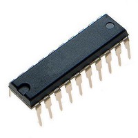
MCHC705JJ7CPE Freescale Semiconductor, MCHC705JJ7CPE Datasheet - Page 92

MCHC705JJ7CPE
Manufacturer Part Number
MCHC705JJ7CPE
Description
IC MCU 8BIT 224 BYTES RAM 20PDIP
Manufacturer
Freescale Semiconductor
Series
HC05r
Datasheet
1.MC705JJ7CDWE.pdf
(164 pages)
Specifications of MCHC705JJ7CPE
Core Processor
HC05
Core Size
8-Bit
Speed
2.1MHz
Connectivity
SIO
Peripherals
POR, Temp Sensor, WDT
Number Of I /o
14
Program Memory Size
6KB (6K x 8)
Program Memory Type
OTP
Ram Size
224 x 8
Voltage - Supply (vcc/vdd)
2.7 V ~ 5.5 V
Data Converters
A/D 4x12b
Oscillator Type
Internal
Operating Temperature
-40°C ~ 85°C
Package / Case
20-DIP (0.300", 7.62mm)
Processor Series
HC705JJ
Core
HC05
Data Bus Width
8 bit
Data Ram Size
224 B
Interface Type
SIOP
Maximum Clock Frequency
2.1 MHz
Number Of Programmable I/os
14
Number Of Timers
2
Maximum Operating Temperature
+ 85 C
Mounting Style
Through Hole
Minimum Operating Temperature
- 40 C
On-chip Adc
12 bit, 4 Channel
Package
20PDIP
Family Name
HC05
Maximum Speed
2.1 MHz
Operating Supply Voltage
3.3|5 V
Lead Free Status / RoHS Status
Lead free / RoHS Compliant
Eeprom Size
-
Lead Free Status / Rohs Status
Details
Analog Subsystem
8.7 Voltage Comparator Features
The two internal comparators can be used as simple voltage comparators if set up as described in
Table
the analog interrupt. Both comparators can also be active in the stop mode, but cannot directly restart the
part. However, the comparators can directly drive PB4 which can then be connected externally to activate
either a port interrupt on the PA0:3 pins or the IRQ/V
8.7.1 Voltage Comparator 1
Voltage comparator 1 is always connected to two of the port B I/O pins. These pins should be configured
as inputs and have their software programmable pulldowns disabled. Also, the negative input of voltage
comparator 1 is connected to the PB3/AN3/TCAP and shared with the input capture function of the 16-bit
programmable timer. Therefore, the timer input capture interrupt should be disabled so that changes in
the voltage on the PB3/AN3/TCAP pin do not cause unwanted input capture interrupts.
The output of comparator 1 can be connected to the port logic driving the PB4/AN4/TCMP/CMP1 pin such
that the output of the comparator is ORed with the PB4 data bit and the OLVL bit from the 16-bit timer.
This capability requires that the OPT bit is set in the COPR at location $1FF0 as in
COE1 bit is set in the ASR at location $001E.
OPT — Optional Features Bit
92
The OPT bit enables two additional features: direct drive by comparator 1 output to PB4 and voltage
offset capability to sample capacitor in analog subsystem.
1 = Optional features enabled
0 = Optional features disabled
8-8. Both comparators can be active in the wait mode and can directly restart the part by means of
Address:
Comparator
Reset:
Read:
Write:
MC68HC705JJ7 • MC68HC705JP7 Advance Information Data Sheet, Rev. 4.1
1
2
$1FF0
EPMSEC
Bit 7
U
Table 8-8. Voltage Comparator Setup Conditions
Figure 8-12. COP and Security Register (COPR)
ISEN = 0
Current
affected
Source
Enable
Not
= Unimplemented
OPT
U
6
Discharge
ISEN = 0
Disable
affected
Device
Not
U
5
U = Unaffected
DDRB2 = 0
DDRB3 = 0
DDRB0 = 0
DDRB1 = 0
Port B Pin
as Inputs
U
4
PP
pin.
U
3
Pulldowns
Port B Pin
PDIB2 = 1
PDIB3 = 1
PDIB0 = 1
PDIB1 = 1
Disabled
U
2
Prog. Timer Input
ICEN = 0
IEDG = 1
Capture
U
affected
1
Source
Not
Figure
Freescale Semiconductor
COPC
Bit 0
U
8-12, and the


