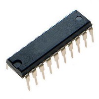
MCHC705JJ7CPE Freescale Semiconductor, MCHC705JJ7CPE Datasheet - Page 140

MCHC705JJ7CPE
Manufacturer Part Number
MCHC705JJ7CPE
Description
IC MCU 8BIT 224 BYTES RAM 20PDIP
Manufacturer
Freescale Semiconductor
Series
HC05r
Datasheet
1.MC705JJ7CDWE.pdf
(164 pages)
Specifications of MCHC705JJ7CPE
Core Processor
HC05
Core Size
8-Bit
Speed
2.1MHz
Connectivity
SIO
Peripherals
POR, Temp Sensor, WDT
Number Of I /o
14
Program Memory Size
6KB (6K x 8)
Program Memory Type
OTP
Ram Size
224 x 8
Voltage - Supply (vcc/vdd)
2.7 V ~ 5.5 V
Data Converters
A/D 4x12b
Oscillator Type
Internal
Operating Temperature
-40°C ~ 85°C
Package / Case
20-DIP (0.300", 7.62mm)
Processor Series
HC705JJ
Core
HC05
Data Bus Width
8 bit
Data Ram Size
224 B
Interface Type
SIOP
Maximum Clock Frequency
2.1 MHz
Number Of Programmable I/os
14
Number Of Timers
2
Maximum Operating Temperature
+ 85 C
Mounting Style
Through Hole
Minimum Operating Temperature
- 40 C
On-chip Adc
12 bit, 4 Channel
Package
20PDIP
Family Name
HC05
Maximum Speed
2.1 MHz
Operating Supply Voltage
3.3|5 V
Lead Free Status / RoHS Status
Lead free / RoHS Compliant
Eeprom Size
-
Lead Free Status / Rohs Status
Details
Electrical Specifications
15.5 Supply Current Characteristics (V
15.6 Supply Current Characteristics (V
140
RUN
WAIT
STOP
Incremental I
RUN
WAIT
STOP
Incremental I
1. V
2. Typical values at midpoint of voltage range, 25°C only
3. Run (Operating) I
4. Wait I
5. Stop I
1. V
2. Typical values at midpoint of voltage range, 25°C only.
3. Run (Operating) I
4. Wait I
5. Stop I
Internal low-power oscillator at 100 kHz
Internal low-power oscillator at 500 kHz
External oscillator running at 4.2 MHz
Internal low-power oscillator at 100 kHz
Internal low-power oscillator at 500 kHz
External oscillator running at 4.2 MHz
Typical
–40°C to 85°C
LVR
Analog subsystem
Internal low-power oscillator at 100 kHz
Internal low-power oscillator at 500 kHz
External oscillator running at 2.1 MHz
Internal low-power oscillator at 100 kHz
Internal low-power oscillator at 500 kHz
External oscillator running at 2.1 MHz
25°C
–40°C to 85°C
LVR
Analog subsystem
inputs 0.2 Vdc from either supply rail (V
inputs 0.2 Vdc from either supply rail (V
DD
DD
(3)
(3)
(4)
(4)
(5)
(5)
= 4.5 to 5.5 Vdc, V
= 2.7 to 3.3 Vdc, V
(analog and LVR disabled)
(analog and LVR disabled)
(analog and LVR disabled)
(analog and LVR disabled)
DD
DD
DD
DD
(analog and LVR disabled)
(analog and LVR disabled)
: All ports configured as inputs, V
: All ports configured as inputs, V
is affected linearly by the OSC2 capacitance.
is affected linearly by the OSC2 capacitance.
DD
DD
for enabled modules
for enabled modules
DD
DD
MC68HC705JJ7 • MC68HC705JP7 Advance Information Data Sheet, Rev. 4.1
, Wait I
, Wait I
Characteristic
Characteristic
SS
SS
= 0 V, T
= 0 V, T
DD
DD
: Measured using external square wave clock source to OSC1 pin or internal oscillator, all
: Measured using external square wave clock source to OSC1 pin or internal oscillator, all
L
L
(1)
(1)
≤ T
≤ T
A
A
DD
DD
≤ T
≤ T
IL
IL
or V
or V
= 0.2 Vdc, V
= 0.2 Vdc, V
H
H
, unless otherwise noted. All values shown reflect average measurements.
, unless otherwise noted. All values shown reflect average measurements.
SS
SS
); no dc loads, less than 50 pF on all outputs, C
); no dc loads, less than 50 pF on all outputs, C
IH
IH
= V
= V
DD
DD
DD
DD
Symbol
Symbol
–0.2 Vdc, OSC1 = V
–0.2 Vdc, OSC1 = V
= 4.5 to 5.5 Vdc)
= 2.7 to 3.3 Vdc)
I
I
I
I
I
I
I
I
DD
DD
DD
DD
DD
DD
DD
DD
Min
Min
—
—
—
—
—
—
—
—
—
—
—
—
—
—
—
—
—
—
—
—
DD
DD
.
.
Typ
Typ
3.00
1.00
1.25
0.50
150
375
380
320
380
45
75
70
20
40
2
4
5
1
2
5
(2)
(2)
L
L
Freescale Semiconductor
= 20 pF on OSC2.
= 20 pF on OSC2.
1100
Max
5.20
2.20
Max
2.60
1.10
568
375
475
320
800
250
475
85
10
20
15
65
10
15
5
Unit
Unit
mA
mA
mA
mA
µA
µA
µA
µA
µA
µA
µA
µA
µA
µA
µA
µA


