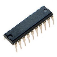
MCHC705JJ7CPE Freescale Semiconductor, MCHC705JJ7CPE Datasheet - Page 82

MCHC705JJ7CPE
Manufacturer Part Number
MCHC705JJ7CPE
Description
IC MCU 8BIT 224 BYTES RAM 20PDIP
Manufacturer
Freescale Semiconductor
Series
HC05r
Datasheet
1.MC705JJ7CDWE.pdf
(164 pages)
Specifications of MCHC705JJ7CPE
Core Processor
HC05
Core Size
8-Bit
Speed
2.1MHz
Connectivity
SIO
Peripherals
POR, Temp Sensor, WDT
Number Of I /o
14
Program Memory Size
6KB (6K x 8)
Program Memory Type
OTP
Ram Size
224 x 8
Voltage - Supply (vcc/vdd)
2.7 V ~ 5.5 V
Data Converters
A/D 4x12b
Oscillator Type
Internal
Operating Temperature
-40°C ~ 85°C
Package / Case
20-DIP (0.300", 7.62mm)
Processor Series
HC705JJ
Core
HC05
Data Bus Width
8 bit
Data Ram Size
224 B
Interface Type
SIOP
Maximum Clock Frequency
2.1 MHz
Number Of Programmable I/os
14
Number Of Timers
2
Maximum Operating Temperature
+ 85 C
Mounting Style
Through Hole
Minimum Operating Temperature
- 40 C
On-chip Adc
12 bit, 4 Channel
Package
20PDIP
Family Name
HC05
Maximum Speed
2.1 MHz
Operating Supply Voltage
3.3|5 V
Lead Free Status / RoHS Status
Lead free / RoHS Compliant
Eeprom Size
-
Lead Free Status / Rohs Status
Details
Analog Subsystem
these bits and the ISEN bit are cleared when the device is reset, the MC68HC705JJ7/MC68HC705JP7
starts with the charge and discharge function disabled.
The length of time required to reach the maximum voltage to be measured and the speed of the time
counting mechanism will determine the resolution of the reading. The time to ramp the external capacitor
voltage to match the maximum voltage is dependent on:
The charging behavior is described by the general equation:
Where:
Since the MCU can measure time in a variety of ways, the resolution of the conversion will depend on the
length of the time keeping function and its prescaling to the oscillator frequency (f
charge time also equals:
Where:
The previous two equations for the charge time, t
for the full scale count (N
Since a given timing method has a fixed charge current and prescaler, then the variation in the resultant
count for a given unknown voltage is mainly dependent on the operating frequency and the capacitance
value used. The desired external capacitance for a given voltage range, f
resolution is defined as:
82
•
•
•
•
•
t
C
V
I
P= Prescaler value (÷ 2, ÷ 4, ÷ 8, etc.)
N= Number of counts during charge time
f
CHG
CHG
OSC
X
EXT
= Unknown voltage (volts)
Charging current to external capacitor
Value of the external capacitor
Clock rate for timing function
Any prescaling of the clock to the timing function
Desired resolution
= Oscillator clock frequency (Hz)
= Charge time (seconds)
= Charge current (µA)
= Capacitance (µF)
Noise on the system ground or the external ramping capacitor can cause
the comparator to trip prematurely. Therefore, in any given application it is
best to use the fastest possible ramp rate (shortest charge time).
The value of any capacitor connected directly to the PB0/AN0 pin should be
limited to less than 2 microfarads. Larger capacitances will create high
discharge currents which may damage the device or create signal noise.
MC68HC705JJ7 • MC68HC705JP7 Advance Information Data Sheet, Rev. 4.1
FS
) of the measured time versus the full scale unknown voltage (V
N
C
FS
EXT
= C
= N
t
CHG
EXT
t
FS
CHG
= C
x V
x P x I
= P x N / f
EXT
CHG
NOTE
NOTE
FS
x f
CHG
, can be combined to form the following expression
x V
OSC
X
/ (V
OSC
/ I
/ (P x I
CHG
FS
x f
CHG
OSC
)
)
OSC
, conversion method, and
OSC
Freescale Semiconductor
). Therefore, the
FS
):


