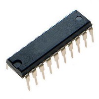
MCHC705JJ7CPE Freescale Semiconductor, MCHC705JJ7CPE Datasheet - Page 67

MCHC705JJ7CPE
Manufacturer Part Number
MCHC705JJ7CPE
Description
IC MCU 8BIT 224 BYTES RAM 20PDIP
Manufacturer
Freescale Semiconductor
Series
HC05r
Datasheet
1.MC705JJ7CDWE.pdf
(164 pages)
Specifications of MCHC705JJ7CPE
Core Processor
HC05
Core Size
8-Bit
Speed
2.1MHz
Connectivity
SIO
Peripherals
POR, Temp Sensor, WDT
Number Of I /o
14
Program Memory Size
6KB (6K x 8)
Program Memory Type
OTP
Ram Size
224 x 8
Voltage - Supply (vcc/vdd)
2.7 V ~ 5.5 V
Data Converters
A/D 4x12b
Oscillator Type
Internal
Operating Temperature
-40°C ~ 85°C
Package / Case
20-DIP (0.300", 7.62mm)
Processor Series
HC705JJ
Core
HC05
Data Bus Width
8 bit
Data Ram Size
224 B
Interface Type
SIOP
Maximum Clock Frequency
2.1 MHz
Number Of Programmable I/os
14
Number Of Timers
2
Maximum Operating Temperature
+ 85 C
Mounting Style
Through Hole
Minimum Operating Temperature
- 40 C
On-chip Adc
12 bit, 4 Channel
Package
20PDIP
Family Name
HC05
Maximum Speed
2.1 MHz
Operating Supply Voltage
3.3|5 V
Lead Free Status / RoHS Status
Lead free / RoHS Compliant
Eeprom Size
-
Lead Free Status / Rohs Status
Details
- Current page: 67 of 164
- Download datasheet (2Mb)
7.4 Port C (28-Pin Versions Only)
Port C is an 8-bit, general-purpose, bidirectional I/O port with these features:
7.4.1 Port C Data Register
The port C data register (PORTC) contains a bit for each of the port C pins. When a port C pin is
programmed to be an output, the state of its data register bit determines the state of the output pin. When
a port C pin is programmed to be an input, reading the port C data register returns the logic state of the pin.
PC7–PC0 — Port C Data Bits
7.4.2 Data Direction Register C
The contents of the port C data direction register (DDRC) determine whether each port C pin is an input
or an output. Writing a logic 1 to a DDRC bit enables the output buffer for the associated port C pin. A
DDRC bit set to a logic 1 also disables the pulldown device for that pin. Writing a logic 0 to a DDRC bit
disables the output buffer for the associated port C pin. A reset initializes all DDRC bits to logic 0s,
configuring all port C pins as inputs.
DDRC7–DDRC0 — Port C Data Direction Bits
Freescale Semiconductor
•
•
•
These read/write bits are software programmable. Data direction of each bit is under the control of the
corresponding bit in the port C data direction register (DDRC). Reset has no effect on port C data.
These read/write bits control port C data direction. Reset clears the DDRC7–DDRC0 bits.
1 = Corresponding port C pin configured as output and pulldown device disabled
0 = Corresponding port C pin configured as input
Individual programmable pulldown devices
High current sinking capability on all port C pins, with a maximum total for port C
High current sourcing capability on all port C pins, with a maximum total for port C
Address:
Address:
Reset:
Reset:
Read:
Read:
Write:
Write:
MC68HC705JJ7 • MC68HC705JP7 Advance Information Data Sheet, Rev. 4.1
$0002
$0006
DDRC7
Bit 7
Bit 7
PC7
0
Figure 7-14. Data Direction Register C (DDRC)
Figure 7-13. Port C Data Register (PORTC)
DDRC6
PC6
6
6
0
DDRC5
PC5
5
5
0
DDRC4
Unaffected by reset
PC4
4
4
0
DDRC3
PC3
3
3
0
DDRC2
PC2
2
2
0
DDRC1
PC1
Port C (28-Pin Versions Only)
1
1
0
DDRC0
Bit 0
Bit 0
PC0
0
67
Related parts for MCHC705JJ7CPE
Image
Part Number
Description
Manufacturer
Datasheet
Request
R
Part Number:
Description:
Manufacturer:
Freescale Semiconductor, Inc
Datasheet:
Part Number:
Description:
Manufacturer:
Freescale Semiconductor, Inc
Datasheet:
Part Number:
Description:
Manufacturer:
Freescale Semiconductor, Inc
Datasheet:
Part Number:
Description:
Manufacturer:
Freescale Semiconductor, Inc
Datasheet:
Part Number:
Description:
Manufacturer:
Freescale Semiconductor, Inc
Datasheet:
Part Number:
Description:
Manufacturer:
Freescale Semiconductor, Inc
Datasheet:
Part Number:
Description:
Manufacturer:
Freescale Semiconductor, Inc
Datasheet:
Part Number:
Description:
Manufacturer:
Freescale Semiconductor, Inc
Datasheet:
Part Number:
Description:
Manufacturer:
Freescale Semiconductor, Inc
Datasheet:
Part Number:
Description:
Manufacturer:
Freescale Semiconductor, Inc
Datasheet:
Part Number:
Description:
Manufacturer:
Freescale Semiconductor, Inc
Datasheet:
Part Number:
Description:
Manufacturer:
Freescale Semiconductor, Inc
Datasheet:
Part Number:
Description:
Manufacturer:
Freescale Semiconductor, Inc
Datasheet:
Part Number:
Description:
Manufacturer:
Freescale Semiconductor, Inc
Datasheet:
Part Number:
Description:
Manufacturer:
Freescale Semiconductor, Inc
Datasheet:


