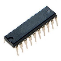
MCHC705JJ7CPE Freescale Semiconductor, MCHC705JJ7CPE Datasheet - Page 79

MCHC705JJ7CPE
Manufacturer Part Number
MCHC705JJ7CPE
Description
IC MCU 8BIT 224 BYTES RAM 20PDIP
Manufacturer
Freescale Semiconductor
Series
HC05r
Datasheet
1.MC705JJ7CDWE.pdf
(164 pages)
Specifications of MCHC705JJ7CPE
Core Processor
HC05
Core Size
8-Bit
Speed
2.1MHz
Connectivity
SIO
Peripherals
POR, Temp Sensor, WDT
Number Of I /o
14
Program Memory Size
6KB (6K x 8)
Program Memory Type
OTP
Ram Size
224 x 8
Voltage - Supply (vcc/vdd)
2.7 V ~ 5.5 V
Data Converters
A/D 4x12b
Oscillator Type
Internal
Operating Temperature
-40°C ~ 85°C
Package / Case
20-DIP (0.300", 7.62mm)
Processor Series
HC705JJ
Core
HC05
Data Bus Width
8 bit
Data Ram Size
224 B
Interface Type
SIOP
Maximum Clock Frequency
2.1 MHz
Number Of Programmable I/os
14
Number Of Timers
2
Maximum Operating Temperature
+ 85 C
Mounting Style
Through Hole
Minimum Operating Temperature
- 40 C
On-chip Adc
12 bit, 4 Channel
Package
20PDIP
Family Name
HC05
Maximum Speed
2.1 MHz
Operating Supply Voltage
3.3|5 V
Lead Free Status / RoHS Status
Lead free / RoHS Compliant
Eeprom Size
-
Lead Free Status / Rohs Status
Details
ISEN
8.4 Analog Status Register
The analog status register (ASR) contains status and control of the comparator flag bits. These bits in the
ASR are shown in
CPF2
CPF1
Freescale Semiconductor
The ISEN enable bit will power down the charge current source and disable the discharge device in
the analog subsystem. Powering down the current source will drop the supply current by about 200
µA. This bit is cleared by a reset of the device.
This read-only flag bit is edge sensitive to the rising output of comparator 2. It is set when the voltage
on the PB0/AN0 pin rises above the voltage on a sample capacitor which creates a positive edge on
the output of comparator 2, regardless of the state of the INV bit in the AMUX register. This bit is reset
by writing a logic 1 to the CPFR2 reset bit in the ASR. This bit is cleared by a reset of the device.
This read-only flag bit is edge sensitive to the rising output of comparator 1. It is set when the voltage
on the PB2/AN2 pin rises above the voltage on the PN3/AN3/TCAP pin which creates a positive edge
on the output of comparator 1, regardless of the state of the INV bit in the AMUX register. This bit is
reset by writing a logic 1 to the CPFR1 reset bit in the ASR. This bit is cleared by a reset of the device.
1 = Writing a logic 1 powers up the ramping current source and enables the discharge device on
0 = Writing a logic 0 powers down the ramping current source and disables the discharge device on
1 = A positive transition on the output of comparator 2 has occurred since the last time the CPF2
0 = A positive transition on the output of comparator 2 has not occurred since the last time the CPF2
1 = A positive transition on the output of comparator 1 has occurred since the last time the CPF1
0 = A positive transition on the output of comparator 1 has not occurred since the last time the CPF1
the PB0/AN0 pin.
the PB0/AN0 pin.
flag has been cleared.
flag has been cleared.
flag has been cleared.
flag has been cleared.
Address:
The analog subsystem has support circuitry which draws current. This
current will be powered down if both comparators and the charge current
source are powered down (ISEN, CP1EN, and CP2EN all cleared).
Powering up either comparator or the charge current source will activate
the support circuitry.
Reset:
Read:
Write:
Figure
MC68HC705JJ7 • MC68HC705JP7 Advance Information Data Sheet, Rev. 4.1
$001E
CPF2
Bit 7
0
8-6. All the bits in this register are cleared by a reset of the device.
Figure 8-6. Analog Status Register (ASR)
= Unimplemented
CPF1
6
0
CPFR2
5
0
0
NOTE
CPFR1
4
0
0
COE1
R
3
0
= Reserved
VOFF
2
0
CMP2
1
0
Analog Status Register
CMP1
Bit 0
R
0
79


