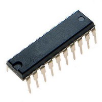
MCHC705JJ7CPE Freescale Semiconductor, MCHC705JJ7CPE Datasheet - Page 46

MCHC705JJ7CPE
Manufacturer Part Number
MCHC705JJ7CPE
Description
IC MCU 8BIT 224 BYTES RAM 20PDIP
Manufacturer
Freescale Semiconductor
Series
HC05r
Datasheet
1.MC705JJ7CDWE.pdf
(164 pages)
Specifications of MCHC705JJ7CPE
Core Processor
HC05
Core Size
8-Bit
Speed
2.1MHz
Connectivity
SIO
Peripherals
POR, Temp Sensor, WDT
Number Of I /o
14
Program Memory Size
6KB (6K x 8)
Program Memory Type
OTP
Ram Size
224 x 8
Voltage - Supply (vcc/vdd)
2.7 V ~ 5.5 V
Data Converters
A/D 4x12b
Oscillator Type
Internal
Operating Temperature
-40°C ~ 85°C
Package / Case
20-DIP (0.300", 7.62mm)
Processor Series
HC705JJ
Core
HC05
Data Bus Width
8 bit
Data Ram Size
224 B
Interface Type
SIOP
Maximum Clock Frequency
2.1 MHz
Number Of Programmable I/os
14
Number Of Timers
2
Maximum Operating Temperature
+ 85 C
Mounting Style
Through Hole
Minimum Operating Temperature
- 40 C
On-chip Adc
12 bit, 4 Channel
Package
20PDIP
Family Name
HC05
Maximum Speed
2.1 MHz
Operating Supply Voltage
3.3|5 V
Lead Free Status / RoHS Status
Lead free / RoHS Compliant
Eeprom Size
-
Lead Free Status / Rohs Status
Details
- Current page: 46 of 164
- Download datasheet (2Mb)
Resets
The LVR reset function can be enabled or disabled by programming the LVREN bit in the MOR.
5.4.4 Illegal Address Reset
An opcode fetch (execution of an instruction) at an address that is not in the EPROM (locations
$0700–$1FFF) or the RAM (locations $0020–$00FF) generates an illegal address reset. The illegal
address reset will assert the pulldown device to pull the RESET pin low for three to four cycles of the
internal bus.
5.5 Reset States
This subsection describe how the various resets initialize the MCU.
5.5.1 CPU
A reset has these effects on the CPU:
5.5.2 I/O Registers
A reset has these effects on input/output (I/O) registers:
5.5.3 Core Timer
A reset has these effects on the core timer:
1. Features related to port C are only available on the 28-pin MC68HC705JP7 devices
46
•
•
•
•
•
•
•
•
•
•
•
•
Loads the stack pointer with $FF
Sets the I bit in the condition code register, inhibiting interrupts
Loads the program counter with the user-defined reset vector from locations $1FFE and $1FFF
Clears the stop latch, enabling the CPU clock
Clears the wait latch, bringing the CPU out of the wait mode
Clears bits in data direction registers configuring pins as inputs:
–
–
–
Clears bits in pulldown inhibit registers to enable pulldown devices:
–
–
–
Has no effect on port A, B, or C
Sets the IRQE bit in the interrupt status and control register (ISCR)
Clears the core timer counter register (CTCR)
Clears the core timer interrupt flag and enable bits in the core timer status and control register
(CTSCR)
Sets the real-time interrupt (RTI) rate selection bits (RT0 and RT1) such that the device will start
with the longest real-time interrupt and longest COP timeout delays
DDRA5–DDRA0 in DDRA for port A
DDRB7–DDRB0 in DDRB for port B
DDRC7–DDRC0 in DDRC for port C
PDIA5–PDIA0 in PDRA for port A
PDIB7–PDIB0 in PDRB for port B
PDICH and PDICL in PDRA for port C
The LVR is intended for applications where the V
normally operates above 4.5 volts.
MC68HC705JJ7 • MC68HC705JP7 Advance Information Data Sheet, Rev. 4.1
(1)
data registers
(1)
(1)
NOTE
DD
supply voltage
Freescale Semiconductor
Related parts for MCHC705JJ7CPE
Image
Part Number
Description
Manufacturer
Datasheet
Request
R
Part Number:
Description:
Manufacturer:
Freescale Semiconductor, Inc
Datasheet:
Part Number:
Description:
Manufacturer:
Freescale Semiconductor, Inc
Datasheet:
Part Number:
Description:
Manufacturer:
Freescale Semiconductor, Inc
Datasheet:
Part Number:
Description:
Manufacturer:
Freescale Semiconductor, Inc
Datasheet:
Part Number:
Description:
Manufacturer:
Freescale Semiconductor, Inc
Datasheet:
Part Number:
Description:
Manufacturer:
Freescale Semiconductor, Inc
Datasheet:
Part Number:
Description:
Manufacturer:
Freescale Semiconductor, Inc
Datasheet:
Part Number:
Description:
Manufacturer:
Freescale Semiconductor, Inc
Datasheet:
Part Number:
Description:
Manufacturer:
Freescale Semiconductor, Inc
Datasheet:
Part Number:
Description:
Manufacturer:
Freescale Semiconductor, Inc
Datasheet:
Part Number:
Description:
Manufacturer:
Freescale Semiconductor, Inc
Datasheet:
Part Number:
Description:
Manufacturer:
Freescale Semiconductor, Inc
Datasheet:
Part Number:
Description:
Manufacturer:
Freescale Semiconductor, Inc
Datasheet:
Part Number:
Description:
Manufacturer:
Freescale Semiconductor, Inc
Datasheet:
Part Number:
Description:
Manufacturer:
Freescale Semiconductor, Inc
Datasheet:


