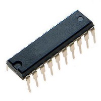
MCHC705JJ7CPE Freescale Semiconductor, MCHC705JJ7CPE Datasheet - Page 96

MCHC705JJ7CPE
Manufacturer Part Number
MCHC705JJ7CPE
Description
IC MCU 8BIT 224 BYTES RAM 20PDIP
Manufacturer
Freescale Semiconductor
Series
HC05r
Datasheet
1.MC705JJ7CDWE.pdf
(164 pages)
Specifications of MCHC705JJ7CPE
Core Processor
HC05
Core Size
8-Bit
Speed
2.1MHz
Connectivity
SIO
Peripherals
POR, Temp Sensor, WDT
Number Of I /o
14
Program Memory Size
6KB (6K x 8)
Program Memory Type
OTP
Ram Size
224 x 8
Voltage - Supply (vcc/vdd)
2.7 V ~ 5.5 V
Data Converters
A/D 4x12b
Oscillator Type
Internal
Operating Temperature
-40°C ~ 85°C
Package / Case
20-DIP (0.300", 7.62mm)
Processor Series
HC705JJ
Core
HC05
Data Bus Width
8 bit
Data Ram Size
224 B
Interface Type
SIOP
Maximum Clock Frequency
2.1 MHz
Number Of Programmable I/os
14
Number Of Timers
2
Maximum Operating Temperature
+ 85 C
Mounting Style
Through Hole
Minimum Operating Temperature
- 40 C
On-chip Adc
12 bit, 4 Channel
Package
20PDIP
Family Name
HC05
Maximum Speed
2.1 MHz
Operating Supply Voltage
3.3|5 V
Lead Free Status / RoHS Status
Lead free / RoHS Compliant
Eeprom Size
-
Lead Free Status / Rohs Status
Details
Simple Synchronous Serial Interface
The SIOP subsystem shares its input/output pins with port B. When the SIOP is enabled (SPE bit set in
the SCR), the port B data direction and data registers are bypassed by the SIOP. The port B data direction
and data registers will remain accessible and can be altered by the application software, but these actions
will not affect the SIOP transmitted or received data.
9.2 SIOP Signal Format
The SIOP subsystem can be software configured for master or slave operation. No external mode
selection inputs are available (for instance, no slave select pin).
9.2.1 Serial Clock (SCK)
The state of the SCK output remains a fixed logic level during idle periods between data transfers. The
edges of SCK indicate the beginning of each output data transfer and latch any incoming data received.
The first bit of transmitted data is output from the SDO pin on the first falling edge of SCK. The first bit of
received data is accepted at the SDI pin on the first rising edge of SCK after the first falling edge. The
transfer is terminated upon the eighth rising edge of SCK.
The idle state of the SCK is determined by the state of the CPHA bit in the SCR. When the CPHA is clear,
SCK will remain idle at a logic 1 as shown in
a logic 0 as shown in
and the SDI latches data in on the rising edge of SCK.
The only difference in the master and slave modes of operation is the sourcing of the SCK. In master
mode, SCK is driven from an internal source within the MCU. In slave mode, SCK is driven from a source
external to the MCU. The SCK frequency is based on one of four divisions of the oscillator clock that is
selected by the SPR0 and SPR1 bits in the SCR.
96
(CPHA = 1)
(CPHA = 0)
SDO
SCK
SDO
SCK
SDI
SDI
MC68HC705JJ7 • MC68HC705JP7 Advance Information Data Sheet, Rev. 4.1
Figure
(IDLE = 0)
Figure 9-2. SIOP Timing Diagram (CPHA = 0)
Figure 9-3. SIOP Timing Diagram (CPHA = 1)
BIT 1
9-3. In both cases, the SDO changes data on the falling edge of the SCK,
BIT 1
BIT 1
BIT 1
100 ns
100 ns
BIT 2
BIT 2
BIT 2
BIT 2
BIT 3
BIT 3
BIT 3
BIT 3
Figure
BIT 4
BIT 4
BIT 4
BIT 4
9-2. When the CPHA is set, SCK will remain idle at
BIT 5
BIT 5
BIT 5
BIT 5
BIT 6
BIT 6
BIT 6
BIT 6
100 ns
100 ns
BIT 7
BIT 7
BIT 7
BIT 7
BIT 8
BIT 8
BIT 8
BIT 8
Freescale Semiconductor
(IDLE = 1)


