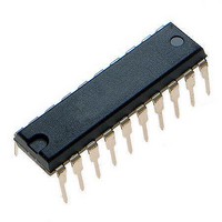
MCHC705JJ7CPE Freescale Semiconductor, MCHC705JJ7CPE Datasheet - Page 40

MCHC705JJ7CPE
Manufacturer Part Number
MCHC705JJ7CPE
Description
IC MCU 8BIT 224 BYTES RAM 20PDIP
Manufacturer
Freescale Semiconductor
Series
HC05r
Datasheet
1.MC705JJ7CDWE.pdf
(164 pages)
Specifications of MCHC705JJ7CPE
Core Processor
HC05
Core Size
8-Bit
Speed
2.1MHz
Connectivity
SIO
Peripherals
POR, Temp Sensor, WDT
Number Of I /o
14
Program Memory Size
6KB (6K x 8)
Program Memory Type
OTP
Ram Size
224 x 8
Voltage - Supply (vcc/vdd)
2.7 V ~ 5.5 V
Data Converters
A/D 4x12b
Oscillator Type
Internal
Operating Temperature
-40°C ~ 85°C
Package / Case
20-DIP (0.300", 7.62mm)
Processor Series
HC705JJ
Core
HC05
Data Bus Width
8 bit
Data Ram Size
224 B
Interface Type
SIOP
Maximum Clock Frequency
2.1 MHz
Number Of Programmable I/os
14
Number Of Timers
2
Maximum Operating Temperature
+ 85 C
Mounting Style
Through Hole
Minimum Operating Temperature
- 40 C
On-chip Adc
12 bit, 4 Channel
Package
20PDIP
Family Name
HC05
Maximum Speed
2.1 MHz
Operating Supply Voltage
3.3|5 V
Lead Free Status / RoHS Status
Lead free / RoHS Compliant
Eeprom Size
-
Lead Free Status / Rohs Status
Details
Interrupts
4.7 Programmable Timer Interrupts
The 16-bit programmable timer can generate an interrupt whenever the following events occur:
Setting the I bit in the condition code register disables timer interrupts. The controls for these interrupts
are in the timer control register (TCR) located at $0012 and in the status bits in the timer status register
(TSR) located at $0013.
4.7.1 Input Capture Interrupt
An input capture interrupt occurs if the input capture flag (ICF) becomes set while the input capture
interrupt enable bit (ICIE) is also set. The ICF flag bit is in the TSR, and the ICIE enable bit is located in
the TCR. The ICF flag bit is cleared by a read of the TSR with the ICF flag bit set, and then followed by a
read of the LSB of the input capture register (ICRL) or by reset. The ICIE enable bit is unaffected by reset.
4.7.2 Output Compare Interrupt
An output compare interrupt occurs if the output compare flag (OCF) becomes set while the output
compare interrupt enable bit (OCIE) is also set. The OCF flag bit is in the TSR and the OCIE enable bit
is in the TCR. The OCF flag bit is cleared by a read of the TSR with the OCF flag bit set, and then followed
by an access to the LSB of the output compare register (OCRL) or by reset. The OCIE enable bit is
unaffected by reset.
4.7.3 Timer Overflow Interrupt
A timer overflow interrupt occurs if the timer overflow flag (TOF) becomes set while the timer overflow
interrupt enable bit (TOIE) is also set. The TOF flag bit is in the TSR and the TOIE enable bit is in the
TCR. The TOF flag bit is cleared by a read of the TSR with the TOF flag bit set, and then followed by an
access to the LSB of the timer registers (TMRL) or by reset. The TOIE enable bit is unaffected by reset.
4.8 Serial Interrupts
The simple serial interface can generate the following interrupts:
Setting the I bit in the condition code register disables serial interrupts. The controls for these interrupts
are in the serial control register (SCR) located at $000A and in the status bits in the serial status register
(SSR) located at $000B.
A transfer complete interrupt occurs if the serial interrupt flag (SPIF) becomes set while the serial interrupt
enable bit (SPIE) is also set. The SPIF flag bit is in the serial status register (SSR) located at $000B, and
the SPIE enable bit is located in the serial control register (SCR) located at $000A. The SPIF flag bit is
cleared by a read of the SSR with the SPIF flag bit set, and then followed by a read or write to the serial
data register (SDR) located at $000C. The SPIF flag bit can also be reset by writing a one to the SPIR bit
in the SCR.
40
•
•
•
•
•
Input capture
Output compare
Timer counter overflow
Receive sequence complete
Transmit sequence complete
MC68HC705JJ7 • MC68HC705JP7 Advance Information Data Sheet, Rev. 4.1
Freescale Semiconductor


