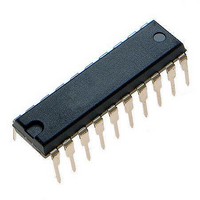
MCHC705JJ7CPE Freescale Semiconductor, MCHC705JJ7CPE Datasheet - Page 121

MCHC705JJ7CPE
Manufacturer Part Number
MCHC705JJ7CPE
Description
IC MCU 8BIT 224 BYTES RAM 20PDIP
Manufacturer
Freescale Semiconductor
Series
HC05r
Datasheet
1.MC705JJ7CDWE.pdf
(164 pages)
Specifications of MCHC705JJ7CPE
Core Processor
HC05
Core Size
8-Bit
Speed
2.1MHz
Connectivity
SIO
Peripherals
POR, Temp Sensor, WDT
Number Of I /o
14
Program Memory Size
6KB (6K x 8)
Program Memory Type
OTP
Ram Size
224 x 8
Voltage - Supply (vcc/vdd)
2.7 V ~ 5.5 V
Data Converters
A/D 4x12b
Oscillator Type
Internal
Operating Temperature
-40°C ~ 85°C
Package / Case
20-DIP (0.300", 7.62mm)
Processor Series
HC705JJ
Core
HC05
Data Bus Width
8 bit
Data Ram Size
224 B
Interface Type
SIOP
Maximum Clock Frequency
2.1 MHz
Number Of Programmable I/os
14
Number Of Timers
2
Maximum Operating Temperature
+ 85 C
Mounting Style
Through Hole
Minimum Operating Temperature
- 40 C
On-chip Adc
12 bit, 4 Channel
Package
20PDIP
Family Name
HC05
Maximum Speed
2.1 MHz
Operating Supply Voltage
3.3|5 V
Lead Free Status / RoHS Status
Lead free / RoHS Compliant
Eeprom Size
-
Lead Free Status / Rohs Status
Details
DELAY — Stop Startup Delay Bit
OSCRES — Oscillator Resistor Bit
SWAIT — STOP Conversion to WAIT Bit
LVREN — Low-Voltage Reset Enable Bit
PIRQ — Port A IRQ Enable Bit
LEVEL — External Interrupt Sensitivity Bit
COPEN — COP Watchdog Enable Bit
Freescale Semiconductor
This EPROM bit selects the number of bus cycles that must elapse before bus activity begins following
a restart from the stop mode.
This EPROM bit configures the internal shunt resistor.
This EPROM bit disables the STOP instruction and prevents inadvertently turning off the COP
watchdog with a STOP instruction. When the SWAIT bit is set, a STOP instruction puts the MCU in
halt mode. Halt mode is a wait-like low-power state. The internal oscillator and timer clock continue to
run, but the CPU clock stops. When the SWAIT bit is clear, a STOP instruction stops the internal
oscillator, the internal clock, the CPU clock, the timer clock, and the COP watchdog timer.
This EPROM bit enables the low-voltage reset (LVR) function.
This EPROM bit enables the PA3–PA0 pins to function as external interrupt sources.
This EPROM bit makes the external interrupt inputs level-triggered as well as edge-triggered
This EPROM bit enables the COP watchdog.
1 = Startup delay is 4064 bus cycles.
0 = Startup delay is 16 bus cycles.
1 = Oscillator configured with 2 M¾ shunt resistor
0 = Oscillator configured without a shunt resistor
1 = STOP instruction converted to WAIT instruction
0 = STOP instruction not converted to WAIT instruction
1 = LVR function enabled
0 = LVR function disabled
1 = PA3–PA0 enabled as external interrupt sources
0 = PA3–PA0 not enabled as external interrupt sources
1 = IRQ/V
0 = IRQ/V
1 = COP watchdog enabled
0 = COP watchdog disabled
PA3–PA0 pins positive-edge triggered and high-level triggered
The 16-cycle delay option will work properly in devices with the internal
low-power oscillator or with a steady external clock source. Check
crystal/ceramic resonator specifications carefully before using the 16-cycle
delay option with a crystal or ceramic resonator.
The optional oscillator resistor is NOT recommended for devices that use
an external RC oscillator. For such devices, this bit should be left erased as
a 0.
PP
PP
MC68HC705JJ7 • MC68HC705JP7 Advance Information Data Sheet, Rev. 4.1
pin negative-edge triggered and low-level triggered;
pin negative-edge triggered only; PA3–PA0 pins positive-edge triggered only
CAUTION
NOTE
EPROM Registers
121


