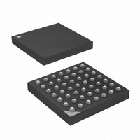
ATXMEGA16A4-CUR Atmel, ATXMEGA16A4-CUR Datasheet - Page 8

ATXMEGA16A4-CUR
Manufacturer Part Number
ATXMEGA16A4-CUR
Description
MCU AVR 16+4KB FLASH 49VFBGA
Manufacturer
Atmel
Series
AVR® XMEGAr
Specifications of ATXMEGA16A4-CUR
Core Processor
AVR
Core Size
8/16-Bit
Speed
32MHz
Connectivity
I²C, IrDA, SPI, UART/USART
Peripherals
Brown-out Detect/Reset, DMA, POR, PWM, WDT
Number Of I /o
34
Program Memory Size
16KB (8K x 16)
Program Memory Type
FLASH
Eeprom Size
1K x 8
Ram Size
2K x 8
Voltage - Supply (vcc/vdd)
1.6 V ~ 3.6 V
Data Converters
A/D 12x12b, D/A 2x12b
Oscillator Type
Internal
Operating Temperature
-40°C ~ 85°C
Package / Case
49-VFBGA
For Use With
ATAVRONEKIT - KIT AVR/AVR32 DEBUGGER/PROGRMMRATSTK600 - DEV KIT FOR AVR/AVR32770-1007 - ISP 4PORT ATMEL AVR MCU SPI/JTAG770-1004 - ISP 4PORT FOR ATMEL AVR MCU SPI
Lead Free Status / RoHS Status
Lead free / RoHS Compliant
Available stocks
Company
Part Number
Manufacturer
Quantity
Price
- Current page: 8 of 445
- Download datasheet (6Mb)
3.6
8077H–AVR–12/09
Instruction Execution Timing
When an enabled interrupt occurs, the Program Counter is vectored to the actual interrupt vector
in order to execute the interrupt handling routine. Hardware clears the corresponding interrupt
flag automatically.
A flexible interrupt controller has dedicated control registers with an additional Global Interrupt
Enable bit in the Status Register. All interrupts have a separate interrupt vector, starting from the
Reset Vector at address 0 in the Program Memory. All interrupts have a programmable interrupt
level. Within each level they have priority in accordance with their interrupt vector position where
the lower interrupt vector address has the higher priority.
The AVR CPU is driven by the CPU clock clk
on page 8
vard architecture and the fast-access Register File concept. This is the basic pipelining concept
to obtain up to 1 MIPS per MHz with the corresponding unique results for functions per cost,
functions per clocks, and functions per power-unit.
Figure 3-2.
Figure 3-3 on page 8
cycle an ALU operation using two register operands is executed, and the result is stored back to
the destination register.
Figure 3-3.
Register Operands Fetch
2nd Instruction Execute
3rd Instruction Execute
ALU Operation Execute
1st Instruction Execute
2nd Instruction Fetch
3rd Instruction Fetch
4th Instruction Fetch
1st Instruction Fetch
Total Execution Time
shows the parallel instruction fetches and instruction executions enabled by the Har-
Result Write Back
The Parallel Instruction Fetches and Instruction Executions
Single Cycle ALU Operation
shows the internal timing concept for the Register File. In a single clock
clk
clk
CPU
CPU
T1
T1
CPU
. No internal clock division is used.
T2
T2
T3
T3
XMEGA A
T4
T4
Figure 3-2
8
Related parts for ATXMEGA16A4-CUR
Image
Part Number
Description
Manufacturer
Datasheet
Request
R

Part Number:
Description:
DEV KIT FOR AVR/AVR32
Manufacturer:
Atmel
Datasheet:

Part Number:
Description:
INTERVAL AND WIPE/WASH WIPER CONTROL IC WITH DELAY
Manufacturer:
ATMEL Corporation
Datasheet:

Part Number:
Description:
Low-Voltage Voice-Switched IC for Hands-Free Operation
Manufacturer:
ATMEL Corporation
Datasheet:

Part Number:
Description:
MONOLITHIC INTEGRATED FEATUREPHONE CIRCUIT
Manufacturer:
ATMEL Corporation
Datasheet:

Part Number:
Description:
AM-FM Receiver IC U4255BM-M
Manufacturer:
ATMEL Corporation
Datasheet:

Part Number:
Description:
Monolithic Integrated Feature Phone Circuit
Manufacturer:
ATMEL Corporation
Datasheet:

Part Number:
Description:
Multistandard Video-IF and Quasi Parallel Sound Processing
Manufacturer:
ATMEL Corporation
Datasheet:

Part Number:
Description:
High-performance EE PLD
Manufacturer:
ATMEL Corporation
Datasheet:

Part Number:
Description:
8-bit Flash Microcontroller
Manufacturer:
ATMEL Corporation
Datasheet:

Part Number:
Description:
2-Wire Serial EEPROM
Manufacturer:
ATMEL Corporation
Datasheet:


