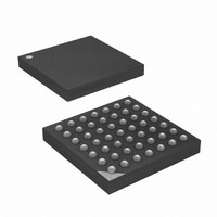
ATXMEGA16A4-CUR Atmel, ATXMEGA16A4-CUR Datasheet - Page 226

ATXMEGA16A4-CUR
Manufacturer Part Number
ATXMEGA16A4-CUR
Description
MCU AVR 16+4KB FLASH 49VFBGA
Manufacturer
Atmel
Series
AVR® XMEGAr
Specifications of ATXMEGA16A4-CUR
Core Processor
AVR
Core Size
8/16-Bit
Speed
32MHz
Connectivity
I²C, IrDA, SPI, UART/USART
Peripherals
Brown-out Detect/Reset, DMA, POR, PWM, WDT
Number Of I /o
34
Program Memory Size
16KB (8K x 16)
Program Memory Type
FLASH
Eeprom Size
1K x 8
Ram Size
2K x 8
Voltage - Supply (vcc/vdd)
1.6 V ~ 3.6 V
Data Converters
A/D 12x12b, D/A 2x12b
Oscillator Type
Internal
Operating Temperature
-40°C ~ 85°C
Package / Case
49-VFBGA
For Use With
ATAVRONEKIT - KIT AVR/AVR32 DEBUGGER/PROGRMMRATSTK600 - DEV KIT FOR AVR/AVR32770-1007 - ISP 4PORT ATMEL AVR MCU SPI/JTAG770-1004 - ISP 4PORT FOR ATMEL AVR MCU SPI
Lead Free Status / RoHS Status
Lead free / RoHS Compliant
Available stocks
Company
Part Number
Manufacturer
Quantity
Price
- Current page: 226 of 445
- Download datasheet (6Mb)
19.10.4
19.10.5
8077H–AVR–12/09
ADDR - TWI Slave Address Register
DATA - TWI Slave Data Register
• Bit 0 - AP: Slave Address or Stop
The Slave Address or Stop (AP) flag indicates whether a valid address or a STOP condition
caused the last setting of the APIF in the STATUS register.
Table 19-8.
This register contains the TWI slave address used by the slave address match logic to deter-
mine if a master has addressed the slave. The 7 most significant bits (ADDR[7:1]) represents the
slave address and the least significant bit (ADDR[0]) is used for general call address recognition.
When ADDR[0] is set this enables general call address recognition logic so the device can
respond to a general address call that addresses all devices on the bus.
When using 10-bit addressing the address match logic only support hardware address recogni-
tion of the first byte of a 10-bit address. By setting ADDR[7:1] = "0b11110nn", 'nn' represents bit
9 and 8 for the slave address. The next byte received is bit 7 to 0 in the 10-bit address, and this
must be handled by software.
When the address match logic detects that a valid address byte is received, the APIF is set, and
the DIR flag is updated.
If the PMEN bit in CTRLA is set, the address match logic responds to all addresses transmitted
on the TWI bus. The ADDR register is not used in this mode.
The data (DATA) register is used when transmitting and received data. During data transfer,
data is shifted from/to the DATA register and to/from the bus. This implies that the DATA register
cannot be accessed during byte transfers, and this is protected in hardware. The Data register
can only be accessed when the SCL line is held low by the slave, i.e. when CLKHOLD is set.
When a master is reading data from the slave, data to send must be written to the DATA regis-
ter. The byte transfer is started when the Master start to clock the data byte from the slave,
followed by the slave receiving the acknowledge bit from the master. The DIF and the CLKHOLD
flag are set.
When a master write data to the slave the DIF and the CLKHOLD flag are set when one byte is
received in the DATA register. If Smart Mode is enabled, reading the DATA register will trigger
the bus operation as set by the ACKACT bit.
Bit
+0x04
Read/Write
Initial Value
Bit
+0x03
Read/Write
Initial Value
AP
0
1
R/W
R/W
TWI slave address or stop
7
0
7
0
Description
A stop condition generated the interrupt on APIF
Address detection generated the interrupt on APIF
R/W
R/W
6
0
6
0
R/W
R/W
5
0
5
0
R/W
R/W
4
0
4
0
ADDR[7:0]
DATA[7:0]
R/W
R/W
3
0
3
0
R/W
R/W
2
0
2
0
R/W
R/W
1
0
1
0
XMEGA A
R/W
R/W
0
0
0
0
ADDR
DATA
226
Related parts for ATXMEGA16A4-CUR
Image
Part Number
Description
Manufacturer
Datasheet
Request
R

Part Number:
Description:
DEV KIT FOR AVR/AVR32
Manufacturer:
Atmel
Datasheet:

Part Number:
Description:
INTERVAL AND WIPE/WASH WIPER CONTROL IC WITH DELAY
Manufacturer:
ATMEL Corporation
Datasheet:

Part Number:
Description:
Low-Voltage Voice-Switched IC for Hands-Free Operation
Manufacturer:
ATMEL Corporation
Datasheet:

Part Number:
Description:
MONOLITHIC INTEGRATED FEATUREPHONE CIRCUIT
Manufacturer:
ATMEL Corporation
Datasheet:

Part Number:
Description:
AM-FM Receiver IC U4255BM-M
Manufacturer:
ATMEL Corporation
Datasheet:

Part Number:
Description:
Monolithic Integrated Feature Phone Circuit
Manufacturer:
ATMEL Corporation
Datasheet:

Part Number:
Description:
Multistandard Video-IF and Quasi Parallel Sound Processing
Manufacturer:
ATMEL Corporation
Datasheet:

Part Number:
Description:
High-performance EE PLD
Manufacturer:
ATMEL Corporation
Datasheet:

Part Number:
Description:
8-bit Flash Microcontroller
Manufacturer:
ATMEL Corporation
Datasheet:

Part Number:
Description:
2-Wire Serial EEPROM
Manufacturer:
ATMEL Corporation
Datasheet:


