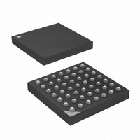
ATXMEGA16A4-CUR Atmel, ATXMEGA16A4-CUR Datasheet - Page 302

ATXMEGA16A4-CUR
Manufacturer Part Number
ATXMEGA16A4-CUR
Description
MCU AVR 16+4KB FLASH 49VFBGA
Manufacturer
Atmel
Series
AVR® XMEGAr
Specifications of ATXMEGA16A4-CUR
Core Processor
AVR
Core Size
8/16-Bit
Speed
32MHz
Connectivity
I²C, IrDA, SPI, UART/USART
Peripherals
Brown-out Detect/Reset, DMA, POR, PWM, WDT
Number Of I /o
34
Program Memory Size
16KB (8K x 16)
Program Memory Type
FLASH
Eeprom Size
1K x 8
Ram Size
2K x 8
Voltage - Supply (vcc/vdd)
1.6 V ~ 3.6 V
Data Converters
A/D 12x12b, D/A 2x12b
Oscillator Type
Internal
Operating Temperature
-40°C ~ 85°C
Package / Case
49-VFBGA
For Use With
ATAVRONEKIT - KIT AVR/AVR32 DEBUGGER/PROGRMMRATSTK600 - DEV KIT FOR AVR/AVR32770-1007 - ISP 4PORT ATMEL AVR MCU SPI/JTAG770-1004 - ISP 4PORT FOR ATMEL AVR MCU SPI
Lead Free Status / RoHS Status
Lead free / RoHS Compliant
Available stocks
Company
Part Number
Manufacturer
Quantity
Price
- Current page: 302 of 445
- Download datasheet (6Mb)
25.16 Register Description - ADC
25.16.1
25.16.2
8077H–AVR–12/09
CTRLA - ADC Control Register A
CTRLB - ADC Control Register B
• Bits 7:6 – DMASEL[1:0]: DMA Request Selection
In addition to giving DMA transfer request for each ADC channel, the ADC can be set up to give
a combined request for all channels. The combined request is decided according to the DMA-
SEL bits. See
Table 25-1.
• Bits 5:2 – CH[3:0]START: ADC Channel Start single conversion
Setting any of these bits will start a conversion on the corresponding ADC channel. Setting sev-
eral bits at the same time will start a conversion sweep on the selected ADC channels, starting
with the channel with lowest number. These bits are cleared by hardware when the conversion
has started.
• Bit 1 – FLUSH: ADC Pipeline Flush:
Setting this bit will flush the ADC pipeline. When this is done the ADC Clock will be restarted on
the next Peripheral clock edge and all conversions in progress are aborted and lost.
After the flush and the ADC Clock restart, the ADC will resume where it left off. I.e. if a channel
sweep was in progress or any conversions was pending, these will enter the ADC pipeline and
complete.
• Bit 0 – ENABLE: ADC Enable
Setting this bit enables the ADC.
• Bits 7:5 - Reserved
These bits are unused and reserved for future use. For compatibility with future devices, always
write these bits to zero when this register is written.
Bit
+0x01
Read/Write
Initial Value
Bit
+0x00
Read/Write
Initial Value
DMASEL[1:0]
00
01
10
11
R/W
7
R
0
-
7
0
Table 25-1
ADC DMA Request Selection
DMASEL[1:0]
R
R/W
6
0
-
6
0
for details.
Group Configuration
R
5
0
R/W
-
5
0
CH0123
CH012
CH01
CONVMODE
OFF
R/W
R/W
4
0
4
0
CH[3:0]START
FREERUN
R/W
R/W
3
0
3
0
Description
No combined DMA request
ADC Channel 0 or 1
ADC Channel 0 or 1 or 2
ADC Channel 0 or 1 or 2 or 3
R/W
R/W
RESOLUTION[1:0]
2
0
2
0
FLUSH
R/W
R/W
1
0
1
0
XMEGA A
ENABLE
R/W
R
0
0
0
0
-
CTRLA
CTRLB
302
Related parts for ATXMEGA16A4-CUR
Image
Part Number
Description
Manufacturer
Datasheet
Request
R

Part Number:
Description:
DEV KIT FOR AVR/AVR32
Manufacturer:
Atmel
Datasheet:

Part Number:
Description:
INTERVAL AND WIPE/WASH WIPER CONTROL IC WITH DELAY
Manufacturer:
ATMEL Corporation
Datasheet:

Part Number:
Description:
Low-Voltage Voice-Switched IC for Hands-Free Operation
Manufacturer:
ATMEL Corporation
Datasheet:

Part Number:
Description:
MONOLITHIC INTEGRATED FEATUREPHONE CIRCUIT
Manufacturer:
ATMEL Corporation
Datasheet:

Part Number:
Description:
AM-FM Receiver IC U4255BM-M
Manufacturer:
ATMEL Corporation
Datasheet:

Part Number:
Description:
Monolithic Integrated Feature Phone Circuit
Manufacturer:
ATMEL Corporation
Datasheet:

Part Number:
Description:
Multistandard Video-IF and Quasi Parallel Sound Processing
Manufacturer:
ATMEL Corporation
Datasheet:

Part Number:
Description:
High-performance EE PLD
Manufacturer:
ATMEL Corporation
Datasheet:

Part Number:
Description:
8-bit Flash Microcontroller
Manufacturer:
ATMEL Corporation
Datasheet:

Part Number:
Description:
2-Wire Serial EEPROM
Manufacturer:
ATMEL Corporation
Datasheet:


