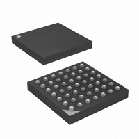
ATXMEGA16A4-CUR Atmel, ATXMEGA16A4-CUR Datasheet - Page 230

ATXMEGA16A4-CUR
Manufacturer Part Number
ATXMEGA16A4-CUR
Description
MCU AVR 16+4KB FLASH 49VFBGA
Manufacturer
Atmel
Series
AVR® XMEGAr
Specifications of ATXMEGA16A4-CUR
Core Processor
AVR
Core Size
8/16-Bit
Speed
32MHz
Connectivity
I²C, IrDA, SPI, UART/USART
Peripherals
Brown-out Detect/Reset, DMA, POR, PWM, WDT
Number Of I /o
34
Program Memory Size
16KB (8K x 16)
Program Memory Type
FLASH
Eeprom Size
1K x 8
Ram Size
2K x 8
Voltage - Supply (vcc/vdd)
1.6 V ~ 3.6 V
Data Converters
A/D 12x12b, D/A 2x12b
Oscillator Type
Internal
Operating Temperature
-40°C ~ 85°C
Package / Case
49-VFBGA
For Use With
ATAVRONEKIT - KIT AVR/AVR32 DEBUGGER/PROGRMMRATSTK600 - DEV KIT FOR AVR/AVR32770-1007 - ISP 4PORT ATMEL AVR MCU SPI/JTAG770-1004 - ISP 4PORT FOR ATMEL AVR MCU SPI
Lead Free Status / RoHS Status
Lead free / RoHS Compliant
Available stocks
Company
Part Number
Manufacturer
Quantity
Price
- Current page: 230 of 445
- Download datasheet (6Mb)
20.3
20.4
8077H–AVR–12/09
Master Mode
Slave Mode
In SPI Slave mode, the control logic will sample the incoming signal of the SCK pin. To ensure
correct sampling of this clock signal, the minimum low and high periods must be:
Low period: longer than 2 CPU clock cycles.
High period: longer than 2 CPU clock cycles.
When the SPI module is enabled, the data direction of the MOSI, MISO, SCK, and SS pins is
overridden according to
from software to have the correct direction according to the application.
Table 20-1.
When configured as a Master, the SPI interface has no automatic control of the SS line. The SS
pin must be configured as output, and controlled by user software. If the bus consists of several
SPI slaves and/or masters, a SPI master can use general I/O pins to control the SS line to each
of the slaves on the bus.
Writing a byte to the Data register starts the SPI clock generator, and the hardware shifts the
eight bits into the selected Slave. After shifting one byte, the SPI clock generator stops and the
SPI Interrupt Flag is set. The Master may continue to shift the next byte by writing new data to
the Data register, or signal the end of transfer by pulling the SS line high. The last incoming byte
will be kept in the Buffer Register.
If the SS pin is configured as an input, it must be held high to ensure Master operation. If the SS
pin is input and being driven low by external circuitry, the SPI module will interpret this as
another master trying to take control of the bus. To avoid bus contention, the Master will take the
following action:
When configured as a Slave, the SPI interface will remain sleeping with MISO tri-stated as long
as the SS pin is driven high. In this state, software may update the contents of the Data register,
but the data will not be shifted out by incoming clock pulses on the SCK pin until the SS pin is
driven low. If SS is driven low and assuming the MISO pin is configured as output, the Slave will
start to shift out data on the first SCK clock pulse. As one byte has been completely shifted, the
SPI Interrupt Flag is set. The Slave may continue to place new data to be sent into the Data reg-
ister before reading the incoming data. The last incoming byte will be kept in the Buffer Register.
When SS is driven high, the SPI logic is reset, and the SPI Slave will not receive any data. Any
partially received packet in the shift register will be dropped.
1. The Master enters Slave mode.
2. The SPI Interrupt Flag is set.
MOSI
MISO
SCK
Pin
SS
Direction, Master SPI
User Defined
Input
User Defined
User Defined
SPI pin overrides
Table
20-1. The pins with user defined direction, must be configured
Direction, Slave SPI
Input
User Defined
Input
Input
XMEGA A
230
Related parts for ATXMEGA16A4-CUR
Image
Part Number
Description
Manufacturer
Datasheet
Request
R

Part Number:
Description:
DEV KIT FOR AVR/AVR32
Manufacturer:
Atmel
Datasheet:

Part Number:
Description:
INTERVAL AND WIPE/WASH WIPER CONTROL IC WITH DELAY
Manufacturer:
ATMEL Corporation
Datasheet:

Part Number:
Description:
Low-Voltage Voice-Switched IC for Hands-Free Operation
Manufacturer:
ATMEL Corporation
Datasheet:

Part Number:
Description:
MONOLITHIC INTEGRATED FEATUREPHONE CIRCUIT
Manufacturer:
ATMEL Corporation
Datasheet:

Part Number:
Description:
AM-FM Receiver IC U4255BM-M
Manufacturer:
ATMEL Corporation
Datasheet:

Part Number:
Description:
Monolithic Integrated Feature Phone Circuit
Manufacturer:
ATMEL Corporation
Datasheet:

Part Number:
Description:
Multistandard Video-IF and Quasi Parallel Sound Processing
Manufacturer:
ATMEL Corporation
Datasheet:

Part Number:
Description:
High-performance EE PLD
Manufacturer:
ATMEL Corporation
Datasheet:

Part Number:
Description:
8-bit Flash Microcontroller
Manufacturer:
ATMEL Corporation
Datasheet:

Part Number:
Description:
2-Wire Serial EEPROM
Manufacturer:
ATMEL Corporation
Datasheet:


