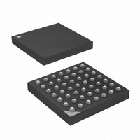
ATXMEGA16A4-CUR Atmel, ATXMEGA16A4-CUR Datasheet - Page 18

ATXMEGA16A4-CUR
Manufacturer Part Number
ATXMEGA16A4-CUR
Description
MCU AVR 16+4KB FLASH 49VFBGA
Manufacturer
Atmel
Series
AVR® XMEGAr
Specifications of ATXMEGA16A4-CUR
Core Processor
AVR
Core Size
8/16-Bit
Speed
32MHz
Connectivity
I²C, IrDA, SPI, UART/USART
Peripherals
Brown-out Detect/Reset, DMA, POR, PWM, WDT
Number Of I /o
34
Program Memory Size
16KB (8K x 16)
Program Memory Type
FLASH
Eeprom Size
1K x 8
Ram Size
2K x 8
Voltage - Supply (vcc/vdd)
1.6 V ~ 3.6 V
Data Converters
A/D 12x12b, D/A 2x12b
Oscillator Type
Internal
Operating Temperature
-40°C ~ 85°C
Package / Case
49-VFBGA
For Use With
ATAVRONEKIT - KIT AVR/AVR32 DEBUGGER/PROGRMMRATSTK600 - DEV KIT FOR AVR/AVR32770-1007 - ISP 4PORT ATMEL AVR MCU SPI/JTAG770-1004 - ISP 4PORT FOR ATMEL AVR MCU SPI
Lead Free Status / RoHS Status
Lead free / RoHS Compliant
Available stocks
Company
Part Number
Manufacturer
Quantity
Price
- Current page: 18 of 445
- Download datasheet (6Mb)
4. Memories
4.1
4.2
8077H–AVR–12/09
Features
Overview
•
•
•
•
This section describes the different memories in XMEGA. The AVR architecture has two main
memory spaces, the Program Memory and the Data Memory. Executable code can only reside
in the Program Memory, while data can be stored both in the Program Memory and the Data
Memory. The Data Memory includes both SRAM, and an EEPROM Memory for non-volatile data
storage. All memory spaces are linear and require no paging. Non-Volatile Memory (NVM)
Flash Program Memory
Data Memory
Production Signature Row Memory for factory programmed data
User Signature Row
– One linear address space
– In-System Programmable
– Self-Programming and Bootloader support
– Application Section for application code
– Application Table Section for application code or data storage
– Boot Section for application code or bootloader code
– Separate lock bits and protection for all sections
– Built in fast CRC check of a selectable flash program memory section
– One linear address space
– Single cycle access from CPU
– SRAM
– EEPROM
– I/O Memory
– External Memory support
– Bus arbitration
– Separate buses for SRAM, EEPROM, I/O Memory and External Memory access
Byte and page accessible
Optional memory mapping for direct load and store
Configuration and Status registers for all peripherals and modules
16 bit-accessible General Purpose Register for global variables or flags
SRAM
SDRAM
Memory mapped external hardware
Safe and deterministic handling of CPU and DMA Controller priority
Simultaneous bus access for CPU and DMA Controller
Device ID for each microcontroller device type
Serial number for each device
Oscillator calibration bytes
ADC, DAC and temperature sensor calibration data
One flash page in size
Can be read and written from software
Content is kept after chip erase
XMEGA A
18
Related parts for ATXMEGA16A4-CUR
Image
Part Number
Description
Manufacturer
Datasheet
Request
R

Part Number:
Description:
DEV KIT FOR AVR/AVR32
Manufacturer:
Atmel
Datasheet:

Part Number:
Description:
INTERVAL AND WIPE/WASH WIPER CONTROL IC WITH DELAY
Manufacturer:
ATMEL Corporation
Datasheet:

Part Number:
Description:
Low-Voltage Voice-Switched IC for Hands-Free Operation
Manufacturer:
ATMEL Corporation
Datasheet:

Part Number:
Description:
MONOLITHIC INTEGRATED FEATUREPHONE CIRCUIT
Manufacturer:
ATMEL Corporation
Datasheet:

Part Number:
Description:
AM-FM Receiver IC U4255BM-M
Manufacturer:
ATMEL Corporation
Datasheet:

Part Number:
Description:
Monolithic Integrated Feature Phone Circuit
Manufacturer:
ATMEL Corporation
Datasheet:

Part Number:
Description:
Multistandard Video-IF and Quasi Parallel Sound Processing
Manufacturer:
ATMEL Corporation
Datasheet:

Part Number:
Description:
High-performance EE PLD
Manufacturer:
ATMEL Corporation
Datasheet:

Part Number:
Description:
8-bit Flash Microcontroller
Manufacturer:
ATMEL Corporation
Datasheet:

Part Number:
Description:
2-Wire Serial EEPROM
Manufacturer:
ATMEL Corporation
Datasheet:


