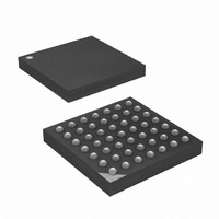
ATXMEGA16A4-CUR Atmel, ATXMEGA16A4-CUR Datasheet - Page 319

ATXMEGA16A4-CUR
Manufacturer Part Number
ATXMEGA16A4-CUR
Description
MCU AVR 16+4KB FLASH 49VFBGA
Manufacturer
Atmel
Series
AVR® XMEGAr
Specifications of ATXMEGA16A4-CUR
Core Processor
AVR
Core Size
8/16-Bit
Speed
32MHz
Connectivity
I²C, IrDA, SPI, UART/USART
Peripherals
Brown-out Detect/Reset, DMA, POR, PWM, WDT
Number Of I /o
34
Program Memory Size
16KB (8K x 16)
Program Memory Type
FLASH
Eeprom Size
1K x 8
Ram Size
2K x 8
Voltage - Supply (vcc/vdd)
1.6 V ~ 3.6 V
Data Converters
A/D 12x12b, D/A 2x12b
Oscillator Type
Internal
Operating Temperature
-40°C ~ 85°C
Package / Case
49-VFBGA
For Use With
ATAVRONEKIT - KIT AVR/AVR32 DEBUGGER/PROGRMMRATSTK600 - DEV KIT FOR AVR/AVR32770-1007 - ISP 4PORT ATMEL AVR MCU SPI/JTAG770-1004 - ISP 4PORT FOR ATMEL AVR MCU SPI
Lead Free Status / RoHS Status
Lead free / RoHS Compliant
Available stocks
Company
Part Number
Manufacturer
Quantity
Price
- Current page: 319 of 445
- Download datasheet (6Mb)
26.6
26.7
26.8
26.9
8077H–AVR–12/09
DAC clock
Timing constraints
Low Power mode
Calibration
Figure 26-2. DAC output model
Notes:
The DAC is clocked from the Peripheral clock (clk
refresh rate in S/H mode is configured relative to the Peripheral Clock.
Some timing constraints are given to make sure the DAC operates correctly. The timing con-
straints are relative to the frequency of the Peripheral clock. Not meeting the timing constraints
may reduce the accuracy of DAC conversions.
To reduce the power consumption in DAC conversions, the DAC may be set in a Low Power
mode. In Low Power mode, the DAC is turned off between each conversion. Conversion time
will be longer if new conversions are started in this mode. To put the DAC into low power mode,
you need to set the bit 1 in CTRLA register (called DACCRA).
To achieve optimal accuracy, it is possible to calibrate both gain and offset error in the DAC.
There is a 7-bit calibration value for gain adjustment and a 7-bit calibration value for offset
adjustment.
To get the best calibration result it is recommended to use the same VREF, output channel
selection, sampling time, and refresh interval when calibrating as will be used in normal DAC
operation. The theoretical transfer function for the DAC was shown in
Including errors, the DAC output value can be expressed as:
In an ideal DAC, gain is 1 and offset is 0.
V
• The DAC sampling time is the time interval between a completed channel conversion until
• The DAC refresh time is the time interval between each time a channel is updated in dual
DAC voltage
DACxX
starting a new conversion. This should not be less than 1 µs for single channel mode and 1.5
µs for dual channel (S/H) mode.
channel mode. This should not be more than 30 µs.
1. The DAC R
2. The DAC R
=
gain
⋅
CHnDATA
--------------------------- -
0xFFF
channel
channel
Buffer
+
is ~300 Ω for ATxmegaA3 and ATxmegaA4
is ~850 Ω for ATxmegaA1
offset
DAC out
PER
) directly. The DAC conversion interval and
R
R
feedback
channel
”Overview” on page
XMEGA A
DAC output
317.
319
Related parts for ATXMEGA16A4-CUR
Image
Part Number
Description
Manufacturer
Datasheet
Request
R

Part Number:
Description:
DEV KIT FOR AVR/AVR32
Manufacturer:
Atmel
Datasheet:

Part Number:
Description:
INTERVAL AND WIPE/WASH WIPER CONTROL IC WITH DELAY
Manufacturer:
ATMEL Corporation
Datasheet:

Part Number:
Description:
Low-Voltage Voice-Switched IC for Hands-Free Operation
Manufacturer:
ATMEL Corporation
Datasheet:

Part Number:
Description:
MONOLITHIC INTEGRATED FEATUREPHONE CIRCUIT
Manufacturer:
ATMEL Corporation
Datasheet:

Part Number:
Description:
AM-FM Receiver IC U4255BM-M
Manufacturer:
ATMEL Corporation
Datasheet:

Part Number:
Description:
Monolithic Integrated Feature Phone Circuit
Manufacturer:
ATMEL Corporation
Datasheet:

Part Number:
Description:
Multistandard Video-IF and Quasi Parallel Sound Processing
Manufacturer:
ATMEL Corporation
Datasheet:

Part Number:
Description:
High-performance EE PLD
Manufacturer:
ATMEL Corporation
Datasheet:

Part Number:
Description:
8-bit Flash Microcontroller
Manufacturer:
ATMEL Corporation
Datasheet:

Part Number:
Description:
2-Wire Serial EEPROM
Manufacturer:
ATMEL Corporation
Datasheet:


