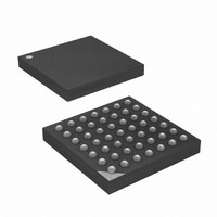
ATXMEGA16A4-CUR Atmel, ATXMEGA16A4-CUR Datasheet - Page 351

ATXMEGA16A4-CUR
Manufacturer Part Number
ATXMEGA16A4-CUR
Description
MCU AVR 16+4KB FLASH 49VFBGA
Manufacturer
Atmel
Series
AVR® XMEGAr
Specifications of ATXMEGA16A4-CUR
Core Processor
AVR
Core Size
8/16-Bit
Speed
32MHz
Connectivity
I²C, IrDA, SPI, UART/USART
Peripherals
Brown-out Detect/Reset, DMA, POR, PWM, WDT
Number Of I /o
34
Program Memory Size
16KB (8K x 16)
Program Memory Type
FLASH
Eeprom Size
1K x 8
Ram Size
2K x 8
Voltage - Supply (vcc/vdd)
1.6 V ~ 3.6 V
Data Converters
A/D 12x12b, D/A 2x12b
Oscillator Type
Internal
Operating Temperature
-40°C ~ 85°C
Package / Case
49-VFBGA
For Use With
ATAVRONEKIT - KIT AVR/AVR32 DEBUGGER/PROGRMMRATSTK600 - DEV KIT FOR AVR/AVR32770-1007 - ISP 4PORT ATMEL AVR MCU SPI/JTAG770-1004 - ISP 4PORT FOR ATMEL AVR MCU SPI
Lead Free Status / RoHS Status
Lead free / RoHS Compliant
Available stocks
Company
Part Number
Manufacturer
Quantity
Price
- Current page: 351 of 445
- Download datasheet (6Mb)
29.4.4
29.4.4.1
29.4.5
8077H–AVR–12/09
Frame Format and Characters
Serial transmission and reception
Special data characters
The JTAG physical layer supports a fixed frame format. A serial frame is defined to be one char-
acter of eight data bits followed by one parity bit.
Figure 29-10. JTAG serial frame format
Table 29-2.
Three data characters are given a special meaning. Common for all three characters is that the
Parity bit is inverted in order to force parity error upon reception. The BREAK character
(0xBB+P1) is used by the External Programmer to force the PDI to abort any on-going operation
and bring the PDI Controller into a known state. The DELAY Character (0xDB+P1) is used by
the PDI to tell the programmer that it has no data ready programmer that it has no transmission
pending (i.e. the PDI is in RX-mode).
Figure 29-11. Special data characters
The JTAG interface supports full duplex communication. At the same time as input data is
shifted in on the TDI pin, output data is shifted out on the TDO pin. However, PDI communica-
tion relies on half duplex data transfer. Dictated by the PDI Controller, the JTAG physical layer
operates in either Transmit- (TX) or Receive- (RX) mode. The available JTAG bit channel is
used for control and status signalling.
The programmer and the JTAG interface operate synchronously on the TCK clock provided by
the programmer. The dependency between the clock edges and data sampling or data change
is fixed. As illustrated in
the falling edge of TCK, while data always should be sampled on the rising edge of TCK.
(0-7)
P
Data/command bits, least significant bit sent first (0 to 7)
Parity bit, even parity is used
Figure 29-10 on page
1
1
1
0
1
1
1
1 EMPTY CHARACTER (EB+P1)
1 BREAK CHARACTER (BB+P1)
1 DELAY CHARACTER (DB+P1)
1
0
0
0
2
1
1
1
3
351, TDI and TDO is always set up (changed) on
1
1
0
FRAME
4
1
0
1
5
0
1
1
6
1
1
1
7
P1
P1
P1
P
XMEGA A
351
Related parts for ATXMEGA16A4-CUR
Image
Part Number
Description
Manufacturer
Datasheet
Request
R

Part Number:
Description:
DEV KIT FOR AVR/AVR32
Manufacturer:
Atmel
Datasheet:

Part Number:
Description:
INTERVAL AND WIPE/WASH WIPER CONTROL IC WITH DELAY
Manufacturer:
ATMEL Corporation
Datasheet:

Part Number:
Description:
Low-Voltage Voice-Switched IC for Hands-Free Operation
Manufacturer:
ATMEL Corporation
Datasheet:

Part Number:
Description:
MONOLITHIC INTEGRATED FEATUREPHONE CIRCUIT
Manufacturer:
ATMEL Corporation
Datasheet:

Part Number:
Description:
AM-FM Receiver IC U4255BM-M
Manufacturer:
ATMEL Corporation
Datasheet:

Part Number:
Description:
Monolithic Integrated Feature Phone Circuit
Manufacturer:
ATMEL Corporation
Datasheet:

Part Number:
Description:
Multistandard Video-IF and Quasi Parallel Sound Processing
Manufacturer:
ATMEL Corporation
Datasheet:

Part Number:
Description:
High-performance EE PLD
Manufacturer:
ATMEL Corporation
Datasheet:

Part Number:
Description:
8-bit Flash Microcontroller
Manufacturer:
ATMEL Corporation
Datasheet:

Part Number:
Description:
2-Wire Serial EEPROM
Manufacturer:
ATMEL Corporation
Datasheet:


