PIC18C658-I/L Microchip Technology, PIC18C658-I/L Datasheet - Page 147
PIC18C658-I/L
Manufacturer Part Number
PIC18C658-I/L
Description
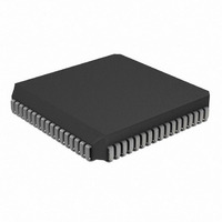
IC PIC MCU OTP 16KX16 68PLCC
Manufacturer
Microchip Technology
Series
PIC® 18Cr
Datasheets
1.PIC16F616T-ISL.pdf
(8 pages)
2.PIC16C770-ISO.pdf
(8 pages)
3.PIC18C658-IPT.pdf
(366 pages)
4.PIC18C658-IPT.pdf
(16 pages)
5.PIC18C658-IPT.pdf
(16 pages)
6.PIC18C658-IPT.pdf
(16 pages)
Specifications of PIC18C658-I/L
Core Size
8-Bit
Program Memory Size
32KB (16K x 16)
Peripherals
Brown-out Detect/Reset, LVD, POR, PWM, WDT
Core Processor
PIC
Speed
40MHz
Connectivity
CAN, I²C, SPI, UART/USART
Number Of I /o
52
Program Memory Type
OTP
Ram Size
1.5K x 8
Voltage - Supply (vcc/vdd)
4.2 V ~ 5.5 V
Data Converters
A/D 12x10b
Oscillator Type
External
Operating Temperature
-40°C ~ 85°C
Package / Case
68-PLCC
Controller Family/series
PIC18
No. Of I/o's
52
Ram Memory Size
1.5KB
Cpu Speed
40MHz
No. Of Timers
4
Processor Series
PIC18C
Core
PIC
Data Bus Width
8 bit
Data Ram Size
1536 B
Interface Type
3-Wire, I2C, SPI, USART, CAN
Maximum Clock Frequency
40 MHz
Number Of Programmable I/os
52
Number Of Timers
4 bit
Operating Supply Voltage
2.5 V to 5.5 V
Maximum Operating Temperature
+ 85 C
Mounting Style
SMD/SMT
3rd Party Development Tools
52715-96, 52716-328, 52717-734, 52712-325, EWPIC18
Development Tools By Supplier
ICE2000, DM163007, DV164136
Minimum Operating Temperature
- 40 C
On-chip Adc
6
Lead Free Status / RoHS Status
Lead free / RoHS Compliant
For Use With
AC164308 - MODULE SKT FOR PM3 68PLCCDVA18PQ640 - DEVICE ADAPT PIC18C658 64-TQFPAC174007 - MODULE SKT PROMATEII 68PLCC
Eeprom Size
-
Lead Free Status / Rohs Status
Details
Other names
PIC18C658IL
Q1162292
Q1162292
Available stocks
Company
Part Number
Manufacturer
Quantity
Price
Company:

Part Number:
PIC18C658-I/L
Manufacturer:
Microchip
Quantity:
385
Company:
Part Number:
PIC18C658-I/L
Manufacturer:
Microchip Technology
Quantity:
10 000
Part Number:
PIC18C658-I/L
Manufacturer:
MICROCHIP/微芯
Quantity:
20 000


15.4
The MSSP module in I
master and slave functions (including general call sup-
port) and provides interrupts on START and STOP bits
in hardware to determine a free bus (Multi-master
mode). The MSSP module implements the standard
mode specifications, as well as 7-bit and 10-bit
addressing.
Two pins are used for data transfer. These are the
RC3/SCK/SCL pin, which is the clock (SCL), and the
RC4/SDI/SDA pin, which is the data (SDA). The user
must configure these pins as inputs or outputs through
the TRISC<4:3> bits.
The MSSP module functions are enabled by setting
MSSP Enable bit SSPEN (SSPCON1 register).
FIGURE 15-6: MSSP BLOCK DIAGRAM
The MSSP module has these six registers for I
ation:
• MSSP Control Register1 (SSPCON1)
• MSSP Control Register2 (SSPCON2)
• MSSP Status Register (SSPSTAT)
• Serial Receive/Transmit Buffer (SSPBUF)
• MSSP Shift Register (SSPSR) - Not directly
• MSSP Address Register (SSPADD)
2000 Microchip Technology Inc.
RC3/SCK/SCL
accessible
RC4/
SDI/
SDA
Note:
MSSP I
I/O pins have diode protection to V
Read
Shift
Clock
2
(I
C Operation
2
MSb
C MODE)
STOP bit detect
2
Match Detect
SSPADD reg
SSPBUF reg
START and
C mode, fully implements all
SSPSR reg
LSb
DD
Write
and V
Internal
Data Bus
(SSPSTAT reg)
Set, RESET
S, P bits
Advanced Information
Addr Match
SS
2
.
C oper-
The SSPCON1 register allows control of the I
ation. The SSPM3:SSPM0 mode selection bits
(SSPCON1 register) allow one of the following I
modes to be selected:
• I
• I
• I
• I
• I
• I
Selection of any I
forces the SCL and SDA pins to be open drain, pro-
vided these pins are programmed to inputs by setting
the appropriate TRISC bits.
15.4.1
In Slave mode, the SCL and SDA pins must be config-
ured as inputs (TRISC<4:3> set). The MSSP module
will override the input state with the output data when
required (slave-transmitter).
When an address is matched, or the data transfer after
an address match is received, the hardware automati-
cally will generate the acknowledge (ACK) pulse and
load the SSPBUF register with the received value cur-
rently in the SSPSR register.
If either or both of the following conditions are true, the
MSSP module will not give this ACK pulse:
a)
b)
In this event, the SSPSR register value is not loaded
into the SSPBUF, but bit SSPIF (PIR registers) is set.
The BF bit is cleared by reading the SSPBUF register,
while bit SSPOV is cleared through software.
The SCL clock input must have a minimum high and
low for proper operation. The high and low times of the
I
MSSP module, is shown in timing parameter #100 and
parameter #101.
2
C specification, as well as the requirement of the
STOP bit interrupts enabled
STOP bit interrupts enabled
is idle
2
2
2
2
2
2
C Master mode, clock = OSC/4 (SSPADD +1)
C Slave mode (7-bit address)
C Slave mode (10-bit address)
C Slave mode (7-bit address), with START and
C Slave mode (10-bit address), with START and
C Firmware controlled master operation, slave
The buffer full bit BF (SSPCON1 register) was
set before the transfer was received.
The overflow bit SSPOV (SSPCON1 register)
was set before the transfer was received.
SLAVE MODE
2
C mode with the SSPEN bit set,
PIC18CXX8
DS30475A-page 147
2
C oper-
2
C
Related parts for PIC18C658-I/L
Image
Part Number
Description
Manufacturer
Datasheet
Request
R

Part Number:
Description:
IC, 8BIT MCU, PIC18F, 40MHZ, LCC-44
Manufacturer:
Microchip Technology
Datasheet:
Part Number:
Description:
IC, 8BIT MCU, PIC18LF, 40MHZ, PLCC-64
Manufacturer:
Microchip Technology
Datasheet:
Part Number:
Description:
IC, 8BIT MCU, PIC18F, 64MHZ, TQFP-80
Manufacturer:
Microchip Technology
Datasheet:

Part Number:
Description:
MCU, MPU & DSP Development Tools CAN/LIN PICtail Plus Daughter Board
Manufacturer:
Microchip Technology
Datasheet:

Part Number:
Description:
IC, 8BIT MCU, PIC18F, 64MHZ, DIP-40
Manufacturer:
Microchip Technology
Datasheet:

Part Number:
Description:
IC, 8BIT MCU, PIC18LF, 40MHZ, PLCC-64
Manufacturer:
Microchip Technology
Datasheet:
Part Number:
Description:
IC, 8BIT MCU, PIC18F, 64MHZ, TQFP-64
Manufacturer:
Microchip Technology
Part Number:
Description:
IC, 8BIT MCU, PIC18F, 64MHZ, TQFP-80
Manufacturer:
Microchip Technology

Part Number:
Description:
8KB, Flash, 768bytes-RAM, 36I/O, 8-bit Family,nanowatt XLP 40 UQFN 5x5x0.5mm TUB
Manufacturer:
Microchip Technology
Datasheet:
Part Number:
Description:
8KB, Flash, 768bytes-RAM, 36I/O, 8-bit Family,nanowatt XLP 40 UQFN 5x5x0.5mm TUB
Manufacturer:
Microchip Technology
Part Number:
Description:
16KB, Flash, 768bytes-RAM, 36I/O, 8-bit Family,nanowatt XLP 40 UQFN 5x5x0.5mm TU
Manufacturer:
Microchip Technology
Datasheet:
Part Number:
Description:
16KB, Flash, 768bytes-RAM, 36I/O, 8-bit Family,nanowatt XLP 40 UQFN 5x5x0.5mm TU
Manufacturer:
Microchip Technology
Part Number:
Description:
32KB, Flash, 1536bytes-RAM, 36I/O, 8-bit Family,nanowatt XLP 40 UQFN 5x5x0.5mm T
Manufacturer:
Microchip Technology
Datasheet:
Part Number:
Description:
32KB, Flash, 1536bytes-RAM, 36I/O, 8-bit Family,nanowatt XLP 40 UQFN 5x5x0.5mm T
Manufacturer:
Microchip Technology
Part Number:
Description:
64KB, Flash, 3968bytes-RAM, 36I/O, 8-bit Family,nanowatt XLP 40 UQFN 5x5x0.5mm T
Manufacturer:
Microchip Technology
Datasheet: