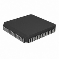
PIC18C658-I/L Microchip Technology, PIC18C658-I/L Datasheet - Page 101

PIC18C658-I/L
Manufacturer Part Number
PIC18C658-I/L
Description
IC PIC MCU OTP 16KX16 68PLCC
Manufacturer
Microchip Technology
Series
PIC® 18Cr
Datasheets
1.PIC16F616T-ISL.pdf
(8 pages)
2.PIC16C770-ISO.pdf
(8 pages)
3.PIC18C658-IPT.pdf
(366 pages)
4.PIC18C658-IPT.pdf
(16 pages)
5.PIC18C658-IPT.pdf
(16 pages)
6.PIC18C658-IPT.pdf
(16 pages)
Specifications of PIC18C658-I/L
Core Size
8-Bit
Program Memory Size
32KB (16K x 16)
Peripherals
Brown-out Detect/Reset, LVD, POR, PWM, WDT
Core Processor
PIC
Speed
40MHz
Connectivity
CAN, I²C, SPI, UART/USART
Number Of I /o
52
Program Memory Type
OTP
Ram Size
1.5K x 8
Voltage - Supply (vcc/vdd)
4.2 V ~ 5.5 V
Data Converters
A/D 12x10b
Oscillator Type
External
Operating Temperature
-40°C ~ 85°C
Package / Case
68-PLCC
Controller Family/series
PIC18
No. Of I/o's
52
Ram Memory Size
1.5KB
Cpu Speed
40MHz
No. Of Timers
4
Processor Series
PIC18C
Core
PIC
Data Bus Width
8 bit
Data Ram Size
1536 B
Interface Type
3-Wire, I2C, SPI, USART, CAN
Maximum Clock Frequency
40 MHz
Number Of Programmable I/os
52
Number Of Timers
4 bit
Operating Supply Voltage
2.5 V to 5.5 V
Maximum Operating Temperature
+ 85 C
Mounting Style
SMD/SMT
3rd Party Development Tools
52715-96, 52716-328, 52717-734, 52712-325, EWPIC18
Development Tools By Supplier
ICE2000, DM163007, DV164136
Minimum Operating Temperature
- 40 C
On-chip Adc
6
Lead Free Status / RoHS Status
Lead free / RoHS Compliant
For Use With
AC164308 - MODULE SKT FOR PM3 68PLCCDVA18PQ640 - DEVICE ADAPT PIC18C658 64-TQFPAC174007 - MODULE SKT PROMATEII 68PLCC
Eeprom Size
-
Lead Free Status / Rohs Status
Details
Other names
PIC18C658IL
Q1162292
Q1162292
Available stocks
Company
Part Number
Manufacturer
Quantity
Price
Company:
Part Number:
PIC18C658-I/L
Manufacturer:
Microchip
Quantity:
385
Company:
Part Number:
PIC18C658-I/L
Manufacturer:
Microchip Technology
Quantity:
10 000
Part Number:
PIC18C658-I/L
Manufacturer:
MICROCHIP/微芯
Quantity:
20 000
- PIC16F616T-ISL PDF datasheet
- PIC16C770-ISO PDF datasheet #2
- PIC18C658-IPT PDF datasheet #3
- PIC18C658-IPT PDF datasheet #4
- PIC18C658-IPT PDF datasheet #5
- PIC18C658-IPT PDF datasheet #6
- Current page: 101 of 366
- Download datasheet (7Mb)
8.7
PORTG is a 5-bit wide, bi-directional port. The corre-
sponding Data Direction register is TRISG. Setting a
TRISG bit (=1) will make the corresponding PORTG pin
an input (i.e., put the corresponding output driver in a
hi-impedance mode). Clearing a TRISG bit (=0) will
make the corresponding PORTG pin an output (i.e., put
the contents of the output latch on the selected pin).
Read-modify-write operations on the LATG register
read and write the latched output value for PORTG.
Pins RG0-RG2 on PORTG are multiplexed with the
CAN peripheral. Refer to "CAN Module", Section 17.0
for proper settings of TRISG when CAN is enabled.
FIGURE 8-12: RG0/CANTX0 PIN BLOCK DIAGRAM
2000 Microchip Technology Inc.
Note:
Data Bus
WR PORTG or
WR LATG
WR TRISG
RD TRISG
RD PORTG
PORTG, LATG, and TRISG Registers
TXD
I/O pins have diode protection to V
TRIS Latch
Data
RD LATG
D
D
CK
CK
Latch
Q
Q
Q
Q
DD
Advanced Information
and V
SS
.
0
1
OPMODE2:OPMODE0 = 000
EXAMPLE 8-7:
CLRF
CLRF
MOVLW
MOVWF
Q
PORTG
LATG
0x04
TRISG
EN
EN
D
V
V
P
N
INITIALIZING PORTG
SS
DD
; Initialize PORTG by
; clearing output
; data latches
; Alternate method
; to clear output
; data latches
; Value used to
; initialize data
; direction
; Set RG1:RG0 as outputs
; RG2 as input
; RG4:RG3 as outputs
PIC18CXX8
ENDRHI
OPMODE2:OPMODE0=000
Schmitt
Trigger
DS30475A-page 101
I/O Pin
Related parts for PIC18C658-I/L
Image
Part Number
Description
Manufacturer
Datasheet
Request
R

Part Number:
Description:
IC, 8BIT MCU, PIC18F, 40MHZ, LCC-44
Manufacturer:
Microchip Technology
Datasheet:

Part Number:
Description:
IC, 8BIT MCU, PIC18LF, 40MHZ, PLCC-64
Manufacturer:
Microchip Technology
Datasheet:

Part Number:
Description:
IC, 8BIT MCU, PIC18F, 64MHZ, TQFP-80
Manufacturer:
Microchip Technology
Datasheet:

Part Number:
Description:
MCU, MPU & DSP Development Tools CAN/LIN PICtail Plus Daughter Board
Manufacturer:
Microchip Technology
Datasheet:

Part Number:
Description:
IC, 8BIT MCU, PIC18F, 64MHZ, DIP-40
Manufacturer:
Microchip Technology
Datasheet:

Part Number:
Description:
IC, 8BIT MCU, PIC18LF, 40MHZ, PLCC-64
Manufacturer:
Microchip Technology
Datasheet:

Part Number:
Description:
IC, 8BIT MCU, PIC18F, 64MHZ, TQFP-64
Manufacturer:
Microchip Technology

Part Number:
Description:
IC, 8BIT MCU, PIC18F, 64MHZ, TQFP-80
Manufacturer:
Microchip Technology

Part Number:
Description:
8KB, Flash, 768bytes-RAM, 36I/O, 8-bit Family,nanowatt XLP 40 UQFN 5x5x0.5mm TUB
Manufacturer:
Microchip Technology
Datasheet:

Part Number:
Description:
8KB, Flash, 768bytes-RAM, 36I/O, 8-bit Family,nanowatt XLP 40 UQFN 5x5x0.5mm TUB
Manufacturer:
Microchip Technology

Part Number:
Description:
16KB, Flash, 768bytes-RAM, 36I/O, 8-bit Family,nanowatt XLP 40 UQFN 5x5x0.5mm TU
Manufacturer:
Microchip Technology
Datasheet:

Part Number:
Description:
16KB, Flash, 768bytes-RAM, 36I/O, 8-bit Family,nanowatt XLP 40 UQFN 5x5x0.5mm TU
Manufacturer:
Microchip Technology

Part Number:
Description:
32KB, Flash, 1536bytes-RAM, 36I/O, 8-bit Family,nanowatt XLP 40 UQFN 5x5x0.5mm T
Manufacturer:
Microchip Technology
Datasheet:

Part Number:
Description:
32KB, Flash, 1536bytes-RAM, 36I/O, 8-bit Family,nanowatt XLP 40 UQFN 5x5x0.5mm T
Manufacturer:
Microchip Technology

Part Number:
Description:
64KB, Flash, 3968bytes-RAM, 36I/O, 8-bit Family,nanowatt XLP 40 UQFN 5x5x0.5mm T
Manufacturer:
Microchip Technology
Datasheet:


