PIC18C658-I/L Microchip Technology, PIC18C658-I/L Datasheet - Page 124
PIC18C658-I/L
Manufacturer Part Number
PIC18C658-I/L
Description
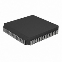
IC PIC MCU OTP 16KX16 68PLCC
Manufacturer
Microchip Technology
Series
PIC® 18Cr
Datasheets
1.PIC16F616T-ISL.pdf
(8 pages)
2.PIC16C770-ISO.pdf
(8 pages)
3.PIC18C658-IPT.pdf
(366 pages)
4.PIC18C658-IPT.pdf
(16 pages)
5.PIC18C658-IPT.pdf
(16 pages)
6.PIC18C658-IPT.pdf
(16 pages)
Specifications of PIC18C658-I/L
Core Size
8-Bit
Program Memory Size
32KB (16K x 16)
Peripherals
Brown-out Detect/Reset, LVD, POR, PWM, WDT
Core Processor
PIC
Speed
40MHz
Connectivity
CAN, I²C, SPI, UART/USART
Number Of I /o
52
Program Memory Type
OTP
Ram Size
1.5K x 8
Voltage - Supply (vcc/vdd)
4.2 V ~ 5.5 V
Data Converters
A/D 12x10b
Oscillator Type
External
Operating Temperature
-40°C ~ 85°C
Package / Case
68-PLCC
Controller Family/series
PIC18
No. Of I/o's
52
Ram Memory Size
1.5KB
Cpu Speed
40MHz
No. Of Timers
4
Processor Series
PIC18C
Core
PIC
Data Bus Width
8 bit
Data Ram Size
1536 B
Interface Type
3-Wire, I2C, SPI, USART, CAN
Maximum Clock Frequency
40 MHz
Number Of Programmable I/os
52
Number Of Timers
4 bit
Operating Supply Voltage
2.5 V to 5.5 V
Maximum Operating Temperature
+ 85 C
Mounting Style
SMD/SMT
3rd Party Development Tools
52715-96, 52716-328, 52717-734, 52712-325, EWPIC18
Development Tools By Supplier
ICE2000, DM163007, DV164136
Minimum Operating Temperature
- 40 C
On-chip Adc
6
Lead Free Status / RoHS Status
Lead free / RoHS Compliant
For Use With
AC164308 - MODULE SKT FOR PM3 68PLCCDVA18PQ640 - DEVICE ADAPT PIC18C658 64-TQFPAC174007 - MODULE SKT PROMATEII 68PLCC
Eeprom Size
-
Lead Free Status / Rohs Status
Details
Other names
PIC18C658IL
Q1162292
Q1162292
Available stocks
Company
Part Number
Manufacturer
Quantity
Price
Company:

Part Number:
PIC18C658-I/L
Manufacturer:
Microchip
Quantity:
385
Company:
Part Number:
PIC18C658-I/L
Manufacturer:
Microchip Technology
Quantity:
10 000
Part Number:
PIC18C658-I/L
Manufacturer:
MICROCHIP/微芯
Quantity:
20 000


PIC18CXX8
13.1
Timer3 can operate in one of these modes:
• As a timer
• As a synchronous counter
• As an asynchronous counter
The operating mode is determined by the clock select
bit, TMR3CS (T3CON register).
FIGURE 13-1: TIMER3 BLOCK DIAGRAM
FIGURE 13-2: TIMER3 BLOCK DIAGRAM CONFIGURED IN 16-BIT READ/WRITE MODE
DS30475A-page 124
TMR3IF Overflow
Interrupt Flag
bit
Note 1:
Note 1:
T1OSO/
T13CKI
T1OSI
Timer3 Operation
Data Bus<7:0>
Write TMR3L
Read TMR3L
T1OSO/
T13CKI
T1OSI
When the T1OSCEN bit is cleared, the inverter and feedback resistor are turned off. This eliminates power drain.
When enable bit T1OSCEN is cleared, the inverter and feedback resistor are turned off. This eliminates power drain.
TMR3IF
Overflow
Interrupt
Flag bit
T1OSC
8
TMR3H
TMR3H
8
To Timer1 Clock Input
TMR3H
T1OSC
Enable
Oscillator
T1OSCEN
8
TMR3
(1)
8
TMR3L
Oscillator
Enable
T1OSCEN
Advanced Information
TMR3L
CLR
(1)
CLR
Internal
Clock
Fosc/4
Clock
F
Internal
TMR3ON
OSC
on/off
TMR3CS
/4
TMR3ON
When TMR3CS = 0, Timer3 increments every instruc-
tion cycle. When TMR3CS = 1, Timer3 increments on
every rising edge of the Timer1 external clock input or
the Timer1 oscillator, if enabled.
When the Timer1 oscillator is enabled (T1OSCEN is
set), the RC1/T1OSI and RC0/T1OSO/T1CKI pins
become inputs. That is, the TRISC<1:0> value is
ignored.
Timer3 also has an internal “RESET input”. This
RESET can be generated by the CCP module
(Section 13.0).
On/Off
1
0
TMR3CS
T3CCPx
CCP Special Trigger
1
0
T3CCPx
T3CKPS1:T3CKPS0
CCP Special Trigger
T3SYNC
T3CKPS1:T3CKPS0
Prescaler
1, 2, 4, 8
T3SYNC
0
1
Prescaler
1, 2, 4, 8
2
0
1
2
2000 Microchip Technology Inc.
Synchronized
Clock Input
Synchronize
SLEEP Input
Synchronized
Clock Input
Synchronize
SLEEP Input
det
det
Related parts for PIC18C658-I/L
Image
Part Number
Description
Manufacturer
Datasheet
Request
R

Part Number:
Description:
IC, 8BIT MCU, PIC18F, 40MHZ, LCC-44
Manufacturer:
Microchip Technology
Datasheet:
Part Number:
Description:
IC, 8BIT MCU, PIC18LF, 40MHZ, PLCC-64
Manufacturer:
Microchip Technology
Datasheet:
Part Number:
Description:
IC, 8BIT MCU, PIC18F, 64MHZ, TQFP-80
Manufacturer:
Microchip Technology
Datasheet:

Part Number:
Description:
MCU, MPU & DSP Development Tools CAN/LIN PICtail Plus Daughter Board
Manufacturer:
Microchip Technology
Datasheet:

Part Number:
Description:
IC, 8BIT MCU, PIC18F, 64MHZ, DIP-40
Manufacturer:
Microchip Technology
Datasheet:

Part Number:
Description:
IC, 8BIT MCU, PIC18LF, 40MHZ, PLCC-64
Manufacturer:
Microchip Technology
Datasheet:
Part Number:
Description:
IC, 8BIT MCU, PIC18F, 64MHZ, TQFP-64
Manufacturer:
Microchip Technology
Part Number:
Description:
IC, 8BIT MCU, PIC18F, 64MHZ, TQFP-80
Manufacturer:
Microchip Technology

Part Number:
Description:
8KB, Flash, 768bytes-RAM, 36I/O, 8-bit Family,nanowatt XLP 40 UQFN 5x5x0.5mm TUB
Manufacturer:
Microchip Technology
Datasheet:
Part Number:
Description:
8KB, Flash, 768bytes-RAM, 36I/O, 8-bit Family,nanowatt XLP 40 UQFN 5x5x0.5mm TUB
Manufacturer:
Microchip Technology
Part Number:
Description:
16KB, Flash, 768bytes-RAM, 36I/O, 8-bit Family,nanowatt XLP 40 UQFN 5x5x0.5mm TU
Manufacturer:
Microchip Technology
Datasheet:
Part Number:
Description:
16KB, Flash, 768bytes-RAM, 36I/O, 8-bit Family,nanowatt XLP 40 UQFN 5x5x0.5mm TU
Manufacturer:
Microchip Technology
Part Number:
Description:
32KB, Flash, 1536bytes-RAM, 36I/O, 8-bit Family,nanowatt XLP 40 UQFN 5x5x0.5mm T
Manufacturer:
Microchip Technology
Datasheet:
Part Number:
Description:
32KB, Flash, 1536bytes-RAM, 36I/O, 8-bit Family,nanowatt XLP 40 UQFN 5x5x0.5mm T
Manufacturer:
Microchip Technology
Part Number:
Description:
64KB, Flash, 3968bytes-RAM, 36I/O, 8-bit Family,nanowatt XLP 40 UQFN 5x5x0.5mm T
Manufacturer:
Microchip Technology
Datasheet: