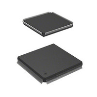
HD6417750RF200DV Renesas Electronics America, HD6417750RF200DV Datasheet - Page 479

HD6417750RF200DV
Manufacturer Part Number
HD6417750RF200DV
Description
MPU 1.5/3.3V 0K I-TEMP PB-FREE 2
Manufacturer
Renesas Electronics America
Series
SuperH® SH7750r
Datasheet
1.D6417750RBP240DV.pdf
(1164 pages)
Specifications of HD6417750RF200DV
Core Processor
SH-4
Core Size
32-Bit
Speed
200MHz
Connectivity
EBI/EMI, FIFO, SCI, SmartCard
Peripherals
DMA, POR, WDT
Number Of I /o
28
Program Memory Type
ROMless
Ram Size
48K x 8
Voltage - Supply (vcc/vdd)
1.35 V ~ 1.6 V
Oscillator Type
External
Operating Temperature
-40°C ~ 85°C
Package / Case
208-QFP Exposed Pad, 208-eQFP, 208-HQFP
Lead Free Status / RoHS Status
Lead free / RoHS Compliant
Eeprom Size
-
Program Memory Size
-
Data Converters
-
Available stocks
Company
Part Number
Manufacturer
Quantity
Price
Company:
Part Number:
HD6417750RF200DV
Manufacturer:
FREESCALE
Quantity:
450
- Current page: 479 of 1164
- Download datasheet (7Mb)
Bits 25 to 23—Area 5 Wait Control (A5W2–A5W0): These bits specify the number of wait
states to be inserted for area 5. For details on MPX interface setting, see table 13.6, MPX Interface
is Selected (Areas 0 to 6).
Bit 25: A5W2
0
1
Bits 22 to 20—Area 5 Burst Pitch (A5B2–A5B0): These bits specify the number of wait states to
be inserted from the second data access onward in a burst transfer with the burst ROM interface
selected.
Bit 22: A5B2
0
1
Bit 24: A5W1
0
1
0
1
Bit 21: A5B1
0
1
0
1
Bit 23: A5W0
0
1
0
1
0
1
0
1
Bit 20: A5B0
0
1
0
1
0
1
0
1
Inserted Wait States
0
1
2
3
6
9
12
15 (Initial value)
Wait States Inserted from Second
Data Access Onward
0
1
2
3
4
5
6
7 (Initial value)
Rev.7.00 Oct. 10, 2008 Page 393 of 1074
Burst Cycle (Excluding First Cycle)
Section 13 Bus State Controller (BSC)
Description
First Cycle
Description
RDY Pin
Ignored
Enabled
Enabled
Enabled
Enabled
Enabled
Enabled
Enabled
REJ09B0366-0700
RDY Pin
Ignored
Enabled
Enabled
Enabled
Enabled
Enabled
Enabled
Enabled
Related parts for HD6417750RF200DV
Image
Part Number
Description
Manufacturer
Datasheet
Request
R

Part Number:
Description:
KIT STARTER FOR M16C/29
Manufacturer:
Renesas Electronics America
Datasheet:

Part Number:
Description:
KIT STARTER FOR R8C/2D
Manufacturer:
Renesas Electronics America
Datasheet:

Part Number:
Description:
R0K33062P STARTER KIT
Manufacturer:
Renesas Electronics America
Datasheet:

Part Number:
Description:
KIT STARTER FOR R8C/23 E8A
Manufacturer:
Renesas Electronics America
Datasheet:

Part Number:
Description:
KIT STARTER FOR R8C/25
Manufacturer:
Renesas Electronics America
Datasheet:

Part Number:
Description:
KIT STARTER H8S2456 SHARPE DSPLY
Manufacturer:
Renesas Electronics America
Datasheet:

Part Number:
Description:
KIT STARTER FOR R8C38C
Manufacturer:
Renesas Electronics America
Datasheet:

Part Number:
Description:
KIT STARTER FOR R8C35C
Manufacturer:
Renesas Electronics America
Datasheet:

Part Number:
Description:
KIT STARTER FOR R8CL3AC+LCD APPS
Manufacturer:
Renesas Electronics America
Datasheet:

Part Number:
Description:
KIT STARTER FOR RX610
Manufacturer:
Renesas Electronics America
Datasheet:

Part Number:
Description:
KIT STARTER FOR R32C/118
Manufacturer:
Renesas Electronics America
Datasheet:

Part Number:
Description:
KIT DEV RSK-R8C/26-29
Manufacturer:
Renesas Electronics America
Datasheet:

Part Number:
Description:
KIT STARTER FOR SH7124
Manufacturer:
Renesas Electronics America
Datasheet:

Part Number:
Description:
KIT STARTER FOR H8SX/1622
Manufacturer:
Renesas Electronics America
Datasheet:

Part Number:
Description:
KIT DEV FOR SH7203
Manufacturer:
Renesas Electronics America
Datasheet:


