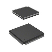
HD6417750RF200DV Renesas Electronics America, HD6417750RF200DV Datasheet - Page 207

HD6417750RF200DV
Manufacturer Part Number
HD6417750RF200DV
Description
MPU 1.5/3.3V 0K I-TEMP PB-FREE 2
Manufacturer
Renesas Electronics America
Series
SuperH® SH7750r
Datasheet
1.D6417750RBP240DV.pdf
(1164 pages)
Specifications of HD6417750RF200DV
Core Processor
SH-4
Core Size
32-Bit
Speed
200MHz
Connectivity
EBI/EMI, FIFO, SCI, SmartCard
Peripherals
DMA, POR, WDT
Number Of I /o
28
Program Memory Type
ROMless
Ram Size
48K x 8
Voltage - Supply (vcc/vdd)
1.35 V ~ 1.6 V
Oscillator Type
External
Operating Temperature
-40°C ~ 85°C
Package / Case
208-QFP Exposed Pad, 208-eQFP, 208-HQFP
Lead Free Status / RoHS Status
Lead free / RoHS Compliant
Eeprom Size
-
Program Memory Size
-
Data Converters
-
Available stocks
Company
Part Number
Manufacturer
Quantity
Price
Company:
Part Number:
HD6417750RF200DV
Manufacturer:
FREESCALE
Quantity:
450
- Current page: 207 of 1164
- Download datasheet (7Mb)
4.3.3
When the OC is enabled (CCR.OCE = 1) and data is written by means of an effective address to a
cacheable area, the cache operates as follows:
1. The tag, V bit, and U bit are read from the cache line indexed by effective address bits [13:5].
2. The tag is compared with bits [28:10] of the address resulting from effective address
3a. Cache hit (copy-back)
3b. Cache hit (write-through)
3c. Cache miss (no copy-back/write-back)
3d. Cache miss (write-through)
translation by the MMU:
A data write in accordance with the access size (quadword/longword/word/byte) is performed
for the data indexed by bits [4:0] of the effective address of the data field of the cache line
indexed by effective address bits [13:5]. Then 1 is set in the U bit.
A data write in accordance with the access size (quadword/longword/word/byte) is performed
for the data indexed by bits [4:0] of the effective address of the data field of the cache line
indexed by effective address bits [13:5]. A write is also performed to the corresponding
external memory using the specified access size.
A data write in accordance with the access size (quadword/longword/word/byte) is performed
for the data indexed by bits [4:0] of the effective address of the data field of the cache line
indexed by effective address bits [13:5]. Then, data is read into the cache line from the external
memory space corresponding to the effective address. Data reading is performed, using the
wraparound method, in order from the longword data corresponding to the effective address,
and one cache line of data is read excluding the written data. During this time, the CPU can
execute the next processing. When reading of one line of data is completed, the tag
corresponding to the effective address is recorded in the cache, and 1 is written to the V bit and
U bit.
A write of the specified access size is performed to the external memory corresponding to the
effective address. In this case, a write to cache is not performed.
• If the tag matches and the V bit is 1
• If the tag matches and the V bit is 0
• If the tag does not match and the V bit is 0
• If the tag does not match, the V bit is 1, and the U bit is 0 → (3c)
• If the tag does not match, the V bit is 1, and the U bit is 1 → (3e)
Write Operation
Rev.7.00 Oct. 10, 2008 Page 121 of 1074
Copy-back
→ (3a)
→ (3c)
→ (3c)
REJ09B0366-0700
Section 4 Caches
Write-through
→ (3b)
→ (3d)
→ (3d)
→ (3d)
→ (3d)
Related parts for HD6417750RF200DV
Image
Part Number
Description
Manufacturer
Datasheet
Request
R

Part Number:
Description:
KIT STARTER FOR M16C/29
Manufacturer:
Renesas Electronics America
Datasheet:

Part Number:
Description:
KIT STARTER FOR R8C/2D
Manufacturer:
Renesas Electronics America
Datasheet:

Part Number:
Description:
R0K33062P STARTER KIT
Manufacturer:
Renesas Electronics America
Datasheet:

Part Number:
Description:
KIT STARTER FOR R8C/23 E8A
Manufacturer:
Renesas Electronics America
Datasheet:

Part Number:
Description:
KIT STARTER FOR R8C/25
Manufacturer:
Renesas Electronics America
Datasheet:

Part Number:
Description:
KIT STARTER H8S2456 SHARPE DSPLY
Manufacturer:
Renesas Electronics America
Datasheet:

Part Number:
Description:
KIT STARTER FOR R8C38C
Manufacturer:
Renesas Electronics America
Datasheet:

Part Number:
Description:
KIT STARTER FOR R8C35C
Manufacturer:
Renesas Electronics America
Datasheet:

Part Number:
Description:
KIT STARTER FOR R8CL3AC+LCD APPS
Manufacturer:
Renesas Electronics America
Datasheet:

Part Number:
Description:
KIT STARTER FOR RX610
Manufacturer:
Renesas Electronics America
Datasheet:

Part Number:
Description:
KIT STARTER FOR R32C/118
Manufacturer:
Renesas Electronics America
Datasheet:

Part Number:
Description:
KIT DEV RSK-R8C/26-29
Manufacturer:
Renesas Electronics America
Datasheet:

Part Number:
Description:
KIT STARTER FOR SH7124
Manufacturer:
Renesas Electronics America
Datasheet:

Part Number:
Description:
KIT STARTER FOR H8SX/1622
Manufacturer:
Renesas Electronics America
Datasheet:

Part Number:
Description:
KIT DEV FOR SH7203
Manufacturer:
Renesas Electronics America
Datasheet:


