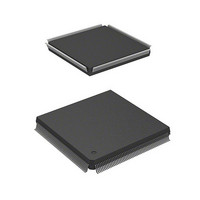
HD6417750RF200DV Renesas Electronics America, HD6417750RF200DV Datasheet - Page 453

HD6417750RF200DV
Manufacturer Part Number
HD6417750RF200DV
Description
MPU 1.5/3.3V 0K I-TEMP PB-FREE 2
Manufacturer
Renesas Electronics America
Series
SuperH® SH7750r
Datasheet
1.D6417750RBP240DV.pdf
(1164 pages)
Specifications of HD6417750RF200DV
Core Processor
SH-4
Core Size
32-Bit
Speed
200MHz
Connectivity
EBI/EMI, FIFO, SCI, SmartCard
Peripherals
DMA, POR, WDT
Number Of I /o
28
Program Memory Type
ROMless
Ram Size
48K x 8
Voltage - Supply (vcc/vdd)
1.35 V ~ 1.6 V
Oscillator Type
External
Operating Temperature
-40°C ~ 85°C
Package / Case
208-QFP Exposed Pad, 208-eQFP, 208-HQFP
Lead Free Status / RoHS Status
Lead free / RoHS Compliant
Eeprom Size
-
Program Memory Size
-
Data Converters
-
Available stocks
Company
Part Number
Manufacturer
Quantity
Price
Company:
Part Number:
HD6417750RF200DV
Manufacturer:
FREESCALE
Quantity:
450
- Current page: 453 of 1164
- Download datasheet (7Mb)
Memory Bus Width: In this LSI, the memory bus width can be set independently for each space.
For area 0, a bus size of 8, 16, 32, or 64 bits can be selected in a power-on reset by the RESET pin,
using external pins. The relationship between the external pins (MD4 and MD3) and the bus width
in a power-on reset is shown below.
MD4
0
1
When SRAM interface or ROM is used in areas 1 to 6, a bus width of 8, 16, 32, or 64 bits can be
selected with bus control register 2 (BCR2). When burst ROM is used, a bus width of 8, 16, 32, or
64* bits can be selected. When byte control SRAM interface is used, a bus width of 16, 32, or 64
bits can be selected. When the MPX interface is used, a bus width of 32 or 64 bits can be selected.
When the DRAM interface is used, a bus width of 16, 32, or 64 bits can be selected with the
Area 3: H'0C000000
Area 0: H'00000000
Area 1: H'04000000
Area 2: H'08000000
Area 4: H'10000000
Area 5: H'14000000
Area 6: H'18000000
6. 64-bit access applies only to transfer by the DMAC. (CHCRn. TS = 000)
7. Settable only for SH7750R.
In a transfer to an external memory by FMOV (FPSCR.SZ = 1), two transfer operations,
each with an access size of 32 bits, are conducted.
MD3
0
1
0
1
Figure 13.3 External Memory Space Allocation
SRAM/synchronous DRAM/DRAM/
MPX
SRAM/burst ROM/MPX
SRAM/MPX/byte control SRAM
SRAM/synchronous DRAM/DRAM/
MPX
SRAM/MPX/byte control SRAM
SRAM/burst ROM/PCMCIA/MPX
SRAM/burst ROM/PCMCIA/MPX
Bus Width
64 bits
8 bits
16 bits
32 bits
Rev.7.00 Oct. 10, 2008 Page 367 of 1074
Section 13 Bus State Controller (BSC)
The PCMCIA interface is
for memory and I/O card use
REJ09B0366-0700
Related parts for HD6417750RF200DV
Image
Part Number
Description
Manufacturer
Datasheet
Request
R

Part Number:
Description:
KIT STARTER FOR M16C/29
Manufacturer:
Renesas Electronics America
Datasheet:

Part Number:
Description:
KIT STARTER FOR R8C/2D
Manufacturer:
Renesas Electronics America
Datasheet:

Part Number:
Description:
R0K33062P STARTER KIT
Manufacturer:
Renesas Electronics America
Datasheet:

Part Number:
Description:
KIT STARTER FOR R8C/23 E8A
Manufacturer:
Renesas Electronics America
Datasheet:

Part Number:
Description:
KIT STARTER FOR R8C/25
Manufacturer:
Renesas Electronics America
Datasheet:

Part Number:
Description:
KIT STARTER H8S2456 SHARPE DSPLY
Manufacturer:
Renesas Electronics America
Datasheet:

Part Number:
Description:
KIT STARTER FOR R8C38C
Manufacturer:
Renesas Electronics America
Datasheet:

Part Number:
Description:
KIT STARTER FOR R8C35C
Manufacturer:
Renesas Electronics America
Datasheet:

Part Number:
Description:
KIT STARTER FOR R8CL3AC+LCD APPS
Manufacturer:
Renesas Electronics America
Datasheet:

Part Number:
Description:
KIT STARTER FOR RX610
Manufacturer:
Renesas Electronics America
Datasheet:

Part Number:
Description:
KIT STARTER FOR R32C/118
Manufacturer:
Renesas Electronics America
Datasheet:

Part Number:
Description:
KIT DEV RSK-R8C/26-29
Manufacturer:
Renesas Electronics America
Datasheet:

Part Number:
Description:
KIT STARTER FOR SH7124
Manufacturer:
Renesas Electronics America
Datasheet:

Part Number:
Description:
KIT STARTER FOR H8SX/1622
Manufacturer:
Renesas Electronics America
Datasheet:

Part Number:
Description:
KIT DEV FOR SH7203
Manufacturer:
Renesas Electronics America
Datasheet:


