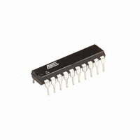
ATTINY2313A-PU Atmel, ATTINY2313A-PU Datasheet - Page 93

ATTINY2313A-PU
Manufacturer Part Number
ATTINY2313A-PU
Description
IC MCU AVR 2K FLASH 20MHZ 20DIP
Manufacturer
Atmel
Series
AVR® ATtinyr
Specifications of ATTINY2313A-PU
Core Processor
AVR
Core Size
8-Bit
Speed
20MHz
Connectivity
I²C, SPI, UART/USART
Peripherals
Brown-out Detect/Reset, POR, PWM, WDT
Number Of I /o
18
Program Memory Size
2KB (1K x 16)
Program Memory Type
FLASH
Eeprom Size
128 x 8
Ram Size
128 x 8
Voltage - Supply (vcc/vdd)
1.8 V ~ 5.5 V
Oscillator Type
Internal
Operating Temperature
-40°C ~ 85°C
Package / Case
20-DIP (0.300", 7.62mm)
Processor Series
ATTINY2x
Core
AVR8
Data Bus Width
8 bit
Data Ram Size
128 B
Interface Type
SPI, USART
Maximum Clock Frequency
20 MHz
Number Of Programmable I/os
18
Operating Supply Voltage
1.8 V to 5.5 V
Maximum Operating Temperature
+ 85 C
Mounting Style
Through Hole
3rd Party Development Tools
EWAVR, EWAVR-BL
Development Tools By Supplier
ATAVRDRAGON, ATSTK500, ATSTK600, ATAVRISP2, ATAVRONEKIT
Minimum Operating Temperature
- 40 C
Controller Family/series
ATtiny
No. Of I/o's
18
Eeprom Memory Size
128Byte
Ram Memory Size
128Byte
Cpu Speed
20MHz
Rohs Compliant
Yes
Lead Free Status / RoHS Status
Lead free / RoHS Compliant
Data Converters
-
Lead Free Status / Rohs Status
Lead free / RoHS Compliant
Available stocks
Company
Part Number
Manufacturer
Quantity
Price
Company:
Part Number:
ATTINY2313A-PU
Manufacturer:
TI
Quantity:
1 560
Part Number:
ATTINY2313A-PU
Manufacturer:
ATMEL/爱特梅尔
Quantity:
20 000
12.5.2
12.5.3
12.6
8246A–AVR–11/09
Output Compare Units
Noise Canceler
Using the Input Capture Unit
Both the Input Capture pin (ICP1) and the Analog Comparator output (ACO) inputs are sampled
using the same technique as for the T1 pin
identical. However, when the noise canceler is enabled, additional logic is inserted before the
edge detector, which increases the delay by four system clock cycles. Note that the input of the
noise canceler and edge detector is always enabled unless the Timer/Counter is set in a Wave-
form Generation mode that uses ICR1 to define TOP.
An Input Capture can be triggered by software by controlling the port of the ICP1 pin.
The noise canceler improves noise immunity by using a simple digital filtering scheme. The
noise canceler input is monitored over four samples, and all four must be equal for changing the
output that in turn is used by the edge detector.
The noise canceler is enabled by setting the Input Capture Noise Canceler (ICNC1) bit in
Timer/Counter Control Register B (TCCR1B). When enabled the noise canceler introduces addi-
tional four system clock cycles of delay from a change applied to the input, to the update of the
ICR1 Register. The noise canceler uses the system clock and is therefore not affected by the
prescaler.
The main challenge when using the Input Capture unit is to assign enough processor capacity
for handling the incoming events. The time between two events is critical. If the processor has
not read the captured value in the ICR1 Register before the next event occurs, the ICR1 will be
overwritten with a new value. In this case the result of the capture will be incorrect.
When using the Input Capture interrupt, the ICR1 Register should be read as early in the inter-
rupt handler routine as possible. Even though the Input Capture interrupt has relatively high
priority, the maximum interrupt response time is dependent on the maximum number of clock
cycles it takes to handle any of the other interrupt requests.
Using the Input Capture unit in any mode of operation when the TOP value (resolution) is
actively changed during operation, is not recommended.
Measurement of an external signal’s duty cycle requires that the trigger edge is changed after
each capture. Changing the edge sensing must be done as early as possible after the ICR1
Register has been read. After a change of the edge, the Input Capture Flag (ICF1) must be
cleared by software (writing a logical one to the I/O bit location). For measuring frequency only,
the clearing of the ICF1 flag is not required (if an interrupt handler is used).
The 16-bit comparator continuously compares TCNT1 with the Output Compare Register
(OCR1x). If TCNT equals OCR1x the comparator signals a match. A match will set the Output
Compare Flag (OCF1x) at the next timer clock cycle. If enabled (OCIE1x = 1), the Output Com-
pare Flag generates an Output Compare interrupt. The OCF1x flag is automatically cleared
when the interrupt is executed. Alternatively the OCF1x flag can be cleared by software by writ-
ing a logical one to its I/O bit location. The Waveform Generator uses the match signal to
generate an output according to operating mode set by the Waveform Generation mode
(WGM13:0) bits and Compare Output mode (COM1x1:0) bits. The TOP and BOTTOM signals
are used by the Waveform Generator for handling the special cases of the extreme values in
some modes of operation
(See “Modes of Operation” on page
(Figure 13-1 on page
96.)
117). The edge detector is also
93


