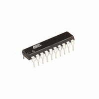
ATTINY2313A-PU Atmel, ATTINY2313A-PU Datasheet - Page 36

ATTINY2313A-PU
Manufacturer Part Number
ATTINY2313A-PU
Description
IC MCU AVR 2K FLASH 20MHZ 20DIP
Manufacturer
Atmel
Series
AVR® ATtinyr
Specifications of ATTINY2313A-PU
Core Processor
AVR
Core Size
8-Bit
Speed
20MHz
Connectivity
I²C, SPI, UART/USART
Peripherals
Brown-out Detect/Reset, POR, PWM, WDT
Number Of I /o
18
Program Memory Size
2KB (1K x 16)
Program Memory Type
FLASH
Eeprom Size
128 x 8
Ram Size
128 x 8
Voltage - Supply (vcc/vdd)
1.8 V ~ 5.5 V
Oscillator Type
Internal
Operating Temperature
-40°C ~ 85°C
Package / Case
20-DIP (0.300", 7.62mm)
Processor Series
ATTINY2x
Core
AVR8
Data Bus Width
8 bit
Data Ram Size
128 B
Interface Type
SPI, USART
Maximum Clock Frequency
20 MHz
Number Of Programmable I/os
18
Operating Supply Voltage
1.8 V to 5.5 V
Maximum Operating Temperature
+ 85 C
Mounting Style
Through Hole
3rd Party Development Tools
EWAVR, EWAVR-BL
Development Tools By Supplier
ATAVRDRAGON, ATSTK500, ATSTK600, ATAVRISP2, ATAVRONEKIT
Minimum Operating Temperature
- 40 C
Controller Family/series
ATtiny
No. Of I/o's
18
Eeprom Memory Size
128Byte
Ram Memory Size
128Byte
Cpu Speed
20MHz
Rohs Compliant
Yes
Lead Free Status / RoHS Status
Lead free / RoHS Compliant
Data Converters
-
Lead Free Status / Rohs Status
Lead free / RoHS Compliant
Available stocks
Company
Part Number
Manufacturer
Quantity
Price
Company:
Part Number:
ATTINY2313A-PU
Manufacturer:
TI
Quantity:
1 560
Part Number:
ATTINY2313A-PU
Manufacturer:
ATMEL/爱特梅尔
Quantity:
20 000
- Current page: 36 of 270
- Download datasheet (7Mb)
7.5
7.5.1
7.5.2
36
Register Description
ATtiny2313A/4313
MCUCR – MCU Control Register
PRR – Power Reduction Register
For analog input pins, the digital input buffer should be disabled at all times. An analog signal
level close to V
input buffers can be disabled by writing to the Digital Input Disable Register (DIDR). See
– Digital Input Disable Register” on page 168
The Sleep Mode Control Register contains control bits for power management.
• Bits 6, 4 – SM1..0: Sleep Mode Select Bits 1 and 0
These bits select between the four available sleep modes as shown in
Table 7-2.
Note:
• Bit 5 – SE: Sleep Enable
The SE bit must be written to logic one to make the MCU enter the sleep mode when the SLEEP
instruction is executed. To avoid the MCU entering the sleep mode unless it is the programmer’s
purpose, it is recommended to write the Sleep Enable (SE) bit to one just before the execution of
the SLEEP instruction and to clear it immediately after waking up.
The Power Reduction Register provides a method to reduce power consumption by allowing
peripheral clock signals to be disabled.
• Bits 7..4 – Res: Reserved Bits
These bits are reserved and will always read zero.
• Bit 3 – PRTIM1: Power Reduction Timer/Counter1
Writing a logic one to this bit shuts down the Timer/Counter1 module. When the Timer/Counter1
is enabled, operation will continue like before the shutdown.
Bit
0x35 (0x55)
Read/Write
Initial Value
Bit
0x06 (0x26)
Read/Write
Initial Value
SM1
0
0
1
1
Standby mode is only recommended for use with external crystals or resonators.
Sleep Mode Select
PUD
R/W
CC
7
0
R
7
–
0
/2 on an input pin can cause significant current even in active mode. Digital
SM0
0
1
0
1
SM1
R/W
6
0
R
6
–
0
Sleep Mode
Idle
Power-down
Standby
Power-down
R/W
SE
5
0
R
5
–
0
SM0
R/W
0
4
R
4
–
0
for details.
ISC11
R/W
3
0
PRTIM1
R/W
3
0
ISC10
R/W
2
0
PRTIM0
R/W
2
0
ISC01
R/W
1
0
PRUSI
Table
R/W
ISC00
1
0
R/W
0
0
7-2.
PRUSART
MCUCR
R/W
0
0
8246A–AVR–11/09
PRR
“DIDR
Related parts for ATTINY2313A-PU
Image
Part Number
Description
Manufacturer
Datasheet
Request
R

Part Number:
Description:
IC, MCU, 8BIT, 2K FLASH, 20SOIC
Manufacturer:
Atmel
Datasheet:

Part Number:
Description:
IC, MCU, 8BIT, 2K FLASH, 20PDIP
Manufacturer:
Atmel
Datasheet:

Part Number:
Description:
IC, MCU, 8BIT, 8K FLASH, 20PDIP
Manufacturer:
Atmel
Datasheet:

Part Number:
Description:
IC, MCU, 8BIT, 8K FLASH, 20SOIC
Manufacturer:
Atmel
Datasheet:

Part Number:
Description:
DEV KIT FOR AVR/AVR32
Manufacturer:
Atmel
Datasheet:

Part Number:
Description:
INTERVAL AND WIPE/WASH WIPER CONTROL IC WITH DELAY
Manufacturer:
ATMEL Corporation
Datasheet:

Part Number:
Description:
Low-Voltage Voice-Switched IC for Hands-Free Operation
Manufacturer:
ATMEL Corporation
Datasheet:

Part Number:
Description:
MONOLITHIC INTEGRATED FEATUREPHONE CIRCUIT
Manufacturer:
ATMEL Corporation
Datasheet:

Part Number:
Description:
AM-FM Receiver IC U4255BM-M
Manufacturer:
ATMEL Corporation
Datasheet:

Part Number:
Description:
Monolithic Integrated Feature Phone Circuit
Manufacturer:
ATMEL Corporation
Datasheet:

Part Number:
Description:
Multistandard Video-IF and Quasi Parallel Sound Processing
Manufacturer:
ATMEL Corporation
Datasheet:

Part Number:
Description:
High-performance EE PLD
Manufacturer:
ATMEL Corporation
Datasheet:


