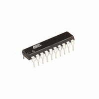
ATTINY2313A-PU Atmel, ATTINY2313A-PU Datasheet - Page 18

ATTINY2313A-PU
Manufacturer Part Number
ATTINY2313A-PU
Description
IC MCU AVR 2K FLASH 20MHZ 20DIP
Manufacturer
Atmel
Series
AVR® ATtinyr
Specifications of ATTINY2313A-PU
Core Processor
AVR
Core Size
8-Bit
Speed
20MHz
Connectivity
I²C, SPI, UART/USART
Peripherals
Brown-out Detect/Reset, POR, PWM, WDT
Number Of I /o
18
Program Memory Size
2KB (1K x 16)
Program Memory Type
FLASH
Eeprom Size
128 x 8
Ram Size
128 x 8
Voltage - Supply (vcc/vdd)
1.8 V ~ 5.5 V
Oscillator Type
Internal
Operating Temperature
-40°C ~ 85°C
Package / Case
20-DIP (0.300", 7.62mm)
Processor Series
ATTINY2x
Core
AVR8
Data Bus Width
8 bit
Data Ram Size
128 B
Interface Type
SPI, USART
Maximum Clock Frequency
20 MHz
Number Of Programmable I/os
18
Operating Supply Voltage
1.8 V to 5.5 V
Maximum Operating Temperature
+ 85 C
Mounting Style
Through Hole
3rd Party Development Tools
EWAVR, EWAVR-BL
Development Tools By Supplier
ATAVRDRAGON, ATSTK500, ATSTK600, ATAVRISP2, ATAVRONEKIT
Minimum Operating Temperature
- 40 C
Controller Family/series
ATtiny
No. Of I/o's
18
Eeprom Memory Size
128Byte
Ram Memory Size
128Byte
Cpu Speed
20MHz
Rohs Compliant
Yes
Lead Free Status / RoHS Status
Lead free / RoHS Compliant
Data Converters
-
Lead Free Status / Rohs Status
Lead free / RoHS Compliant
Available stocks
Company
Part Number
Manufacturer
Quantity
Price
Company:
Part Number:
ATTINY2313A-PU
Manufacturer:
TI
Quantity:
1 560
Part Number:
ATTINY2313A-PU
Manufacturer:
ATMEL/爱特梅尔
Quantity:
20 000
- Current page: 18 of 270
- Download datasheet (7Mb)
5.3.3
5.3.4
5.3.5
18
ATtiny2313A/4313
Split Byte Programming
Erase
Write
EEPMn bits are zero, writing EEPE (within four cycles after EEMPE is written) will trigger the
erase/write operation. Both the erase and write cycle are done in one operation and the total
programming time is given in
and write operations are completed. While the device is busy with programming, it is not possi-
ble to do any other EEPROM operations.
It is possible to split the erase and write cycle in two different operations. This may be useful if
the system requires short access time for some limited period of time (typically if the power sup-
ply voltage falls). In order to take advantage of this method, it is required that the locations to be
written have been erased before the write operation. But since the erase and write operations
are split, it is possible to do the erase operations when the system allows doing time-critical
operations (typically after Power-up).
To erase a byte, the address must be written to EEARL. If the EEPMn bits are 0b01, writing the
EEPE (within four cycles after EEMPE is written) will trigger the erase operation only (program-
ming time is given in
completes. While the device is busy programming, it is not possible to do any other EEPROM
operations.
To write a location, the user must write the address into EEARL and the data into EEDR. If the
EEPMn bits are 0b10, writing the EEPE (within four cycles after EEMPE is written) will trigger
the write operation only (programming time is given in
remains set until the write operation completes. If the location to be written has not been erased
before write, the data that is stored must be considered as lost. While the device is busy with
programming, it is not possible to do any other EEPROM operations.
The calibrated Oscillator is used to time the EEPROM accesses. Make sure the Oscillator fre-
quency is within the requirements described in
page
30.
Table 5-1 on page
Table 5-1 on page
22). The EEPE bit remains set until the erase operation
“OSCCAL – Oscillator Calibration Register” on
22. The EEPE bit remains set until the erase
Table 5-1 on page
22). The EEPE bit
8246A–AVR–11/09
Related parts for ATTINY2313A-PU
Image
Part Number
Description
Manufacturer
Datasheet
Request
R

Part Number:
Description:
IC, MCU, 8BIT, 2K FLASH, 20SOIC
Manufacturer:
Atmel
Datasheet:

Part Number:
Description:
IC, MCU, 8BIT, 2K FLASH, 20PDIP
Manufacturer:
Atmel
Datasheet:

Part Number:
Description:
IC, MCU, 8BIT, 8K FLASH, 20PDIP
Manufacturer:
Atmel
Datasheet:

Part Number:
Description:
IC, MCU, 8BIT, 8K FLASH, 20SOIC
Manufacturer:
Atmel
Datasheet:

Part Number:
Description:
DEV KIT FOR AVR/AVR32
Manufacturer:
Atmel
Datasheet:

Part Number:
Description:
INTERVAL AND WIPE/WASH WIPER CONTROL IC WITH DELAY
Manufacturer:
ATMEL Corporation
Datasheet:

Part Number:
Description:
Low-Voltage Voice-Switched IC for Hands-Free Operation
Manufacturer:
ATMEL Corporation
Datasheet:

Part Number:
Description:
MONOLITHIC INTEGRATED FEATUREPHONE CIRCUIT
Manufacturer:
ATMEL Corporation
Datasheet:

Part Number:
Description:
AM-FM Receiver IC U4255BM-M
Manufacturer:
ATMEL Corporation
Datasheet:

Part Number:
Description:
Monolithic Integrated Feature Phone Circuit
Manufacturer:
ATMEL Corporation
Datasheet:

Part Number:
Description:
Multistandard Video-IF and Quasi Parallel Sound Processing
Manufacturer:
ATMEL Corporation
Datasheet:

Part Number:
Description:
High-performance EE PLD
Manufacturer:
ATMEL Corporation
Datasheet:


