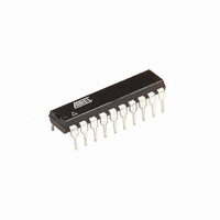
ATTINY2313A-PU Atmel, ATTINY2313A-PU Datasheet - Page 17

ATTINY2313A-PU
Manufacturer Part Number
ATTINY2313A-PU
Description
IC MCU AVR 2K FLASH 20MHZ 20DIP
Manufacturer
Atmel
Series
AVR® ATtinyr
Specifications of ATTINY2313A-PU
Core Processor
AVR
Core Size
8-Bit
Speed
20MHz
Connectivity
I²C, SPI, UART/USART
Peripherals
Brown-out Detect/Reset, POR, PWM, WDT
Number Of I /o
18
Program Memory Size
2KB (1K x 16)
Program Memory Type
FLASH
Eeprom Size
128 x 8
Ram Size
128 x 8
Voltage - Supply (vcc/vdd)
1.8 V ~ 5.5 V
Oscillator Type
Internal
Operating Temperature
-40°C ~ 85°C
Package / Case
20-DIP (0.300", 7.62mm)
Processor Series
ATTINY2x
Core
AVR8
Data Bus Width
8 bit
Data Ram Size
128 B
Interface Type
SPI, USART
Maximum Clock Frequency
20 MHz
Number Of Programmable I/os
18
Operating Supply Voltage
1.8 V to 5.5 V
Maximum Operating Temperature
+ 85 C
Mounting Style
Through Hole
3rd Party Development Tools
EWAVR, EWAVR-BL
Development Tools By Supplier
ATAVRDRAGON, ATSTK500, ATSTK600, ATAVRISP2, ATAVRONEKIT
Minimum Operating Temperature
- 40 C
Controller Family/series
ATtiny
No. Of I/o's
18
Eeprom Memory Size
128Byte
Ram Memory Size
128Byte
Cpu Speed
20MHz
Rohs Compliant
Yes
Lead Free Status / RoHS Status
Lead free / RoHS Compliant
Data Converters
-
Lead Free Status / Rohs Status
Lead free / RoHS Compliant
Available stocks
Company
Part Number
Manufacturer
Quantity
Price
Company:
Part Number:
ATTINY2313A-PU
Manufacturer:
TI
Quantity:
1 560
Part Number:
ATTINY2313A-PU
Manufacturer:
ATMEL/爱特梅尔
Quantity:
20 000
- Current page: 17 of 270
- Download datasheet (7Mb)
5.3
5.3.1
5.3.2
8246A–AVR–11/09
EEPROM Data Memory
EEPROM Read/Write Access
Atomic Byte Programming
Figure 5-3.
The ATtiny2313A/4313 contains 128/256 bytes of data EEPROM memory. It is organized as a
separate data space, in which single bytes can be read and written. The EEPROM has an
endurance of at least 100,000 write/erase cycles. The access between the EEPROM and the
CPU is described in the following, specifying the EEPROM Address Registers, the EEPROM
Data Register, and the EEPROM Control Register. For a detailed description of Serial data
downloading to the EEPROM, see
The EEPROM Access Registers are accessible in the I/O space.
The write access times for the EEPROM are given in
tion, however, lets the user software detect when the next byte can be written. If the user code
contains instructions that write the EEPROM, some precautions must be taken. In heavily fil-
tered power supplies, V
device for some period of time to run at a voltage lower than specified as minimum for the clock
frequency used. See
problems in these situations.
In order to prevent unintentional EEPROM writes, a specific write procedure must be followed.
Refer to
details on this.
When the EEPROM is read, the CPU is halted for four clock cycles before the next instruction is
executed. When the EEPROM is written, the CPU is halted for two clock cycles before the next
instruction is executed.
Using Atomic Byte Programming is the simplest mode. When writing a byte to the EEPROM, the
user must write the address into the EEARL Register and data into EEDR Register. If the
“Atomic Byte Programming” on page 17
Address
clk
On-chip Data SRAM Access Cycles
Data
Data
WR
CPU
RD
“Preventing EEPROM Corruption” on page 20
CC
Compute Address
is likely to rise or fall slowly on Power-up/down. This causes the
T1
Memory Access Instruction
page
190.
Address valid
and
T2
Table 5-1 on page
“Split Byte Programming” on page 18
Next Instruction
for details on how to avoid
T3
22. A self-timing func-
for
17
Related parts for ATTINY2313A-PU
Image
Part Number
Description
Manufacturer
Datasheet
Request
R

Part Number:
Description:
IC, MCU, 8BIT, 2K FLASH, 20SOIC
Manufacturer:
Atmel
Datasheet:

Part Number:
Description:
IC, MCU, 8BIT, 2K FLASH, 20PDIP
Manufacturer:
Atmel
Datasheet:

Part Number:
Description:
IC, MCU, 8BIT, 8K FLASH, 20PDIP
Manufacturer:
Atmel
Datasheet:

Part Number:
Description:
IC, MCU, 8BIT, 8K FLASH, 20SOIC
Manufacturer:
Atmel
Datasheet:

Part Number:
Description:
DEV KIT FOR AVR/AVR32
Manufacturer:
Atmel
Datasheet:

Part Number:
Description:
INTERVAL AND WIPE/WASH WIPER CONTROL IC WITH DELAY
Manufacturer:
ATMEL Corporation
Datasheet:

Part Number:
Description:
Low-Voltage Voice-Switched IC for Hands-Free Operation
Manufacturer:
ATMEL Corporation
Datasheet:

Part Number:
Description:
MONOLITHIC INTEGRATED FEATUREPHONE CIRCUIT
Manufacturer:
ATMEL Corporation
Datasheet:

Part Number:
Description:
AM-FM Receiver IC U4255BM-M
Manufacturer:
ATMEL Corporation
Datasheet:

Part Number:
Description:
Monolithic Integrated Feature Phone Circuit
Manufacturer:
ATMEL Corporation
Datasheet:

Part Number:
Description:
Multistandard Video-IF and Quasi Parallel Sound Processing
Manufacturer:
ATMEL Corporation
Datasheet:

Part Number:
Description:
High-performance EE PLD
Manufacturer:
ATMEL Corporation
Datasheet:


