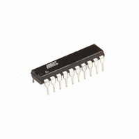
ATTINY2313A-PU Atmel, ATTINY2313A-PU Datasheet - Page 182

ATTINY2313A-PU
Manufacturer Part Number
ATTINY2313A-PU
Description
IC MCU AVR 2K FLASH 20MHZ 20DIP
Manufacturer
Atmel
Series
AVR® ATtinyr
Specifications of ATTINY2313A-PU
Core Processor
AVR
Core Size
8-Bit
Speed
20MHz
Connectivity
I²C, SPI, UART/USART
Peripherals
Brown-out Detect/Reset, POR, PWM, WDT
Number Of I /o
18
Program Memory Size
2KB (1K x 16)
Program Memory Type
FLASH
Eeprom Size
128 x 8
Ram Size
128 x 8
Voltage - Supply (vcc/vdd)
1.8 V ~ 5.5 V
Oscillator Type
Internal
Operating Temperature
-40°C ~ 85°C
Package / Case
20-DIP (0.300", 7.62mm)
Processor Series
ATTINY2x
Core
AVR8
Data Bus Width
8 bit
Data Ram Size
128 B
Interface Type
SPI, USART
Maximum Clock Frequency
20 MHz
Number Of Programmable I/os
18
Operating Supply Voltage
1.8 V to 5.5 V
Maximum Operating Temperature
+ 85 C
Mounting Style
Through Hole
3rd Party Development Tools
EWAVR, EWAVR-BL
Development Tools By Supplier
ATAVRDRAGON, ATSTK500, ATSTK600, ATAVRISP2, ATAVRONEKIT
Minimum Operating Temperature
- 40 C
Controller Family/series
ATtiny
No. Of I/o's
18
Eeprom Memory Size
128Byte
Ram Memory Size
128Byte
Cpu Speed
20MHz
Rohs Compliant
Yes
Lead Free Status / RoHS Status
Lead free / RoHS Compliant
Data Converters
-
Lead Free Status / Rohs Status
Lead free / RoHS Compliant
Available stocks
Company
Part Number
Manufacturer
Quantity
Price
Company:
Part Number:
ATTINY2313A-PU
Manufacturer:
TI
Quantity:
1 560
Part Number:
ATTINY2313A-PU
Manufacturer:
ATMEL/爱特梅尔
Quantity:
20 000
- Current page: 182 of 270
- Download datasheet (7Mb)
20.5
20.5.1
182
Parallel Programming Parameters, Pin Mapping, and Commands
ATtiny2313A/4313
Signal Names
This section describes how to parallel program and verify Flash Program memory, EEPROM
Data memory, Memory Lock bits, and Fuse bits in the ATtiny2313A/4313. Pulses are assumed
to be at least 250 ns unless otherwise noted.
In this section, some pins of the ATtiny2313A/4313 are referenced by signal names describing
their functionality during parallel programming, see
Pins not described in the following table are referenced by pin names.
Figure 20-1. Parallel Programming
Table 20-9.
The XA1/XA0 pins determine the action executed when the XTAL1 pin is given a positive pulse.
The bit coding is shown in
Signal Name in
Programming
BS1/PAGEL
RDY/BSY
XA1/BS2
DATA I/O
Mode
XA0
WR
OE
Pin Name Mapping
PB7-0
Name
PD1
PD2
PD3
PD4
PD5
PD6
Pin
BS1/PAGEL
RDY/BSY
XA1/BS2
Table 20-11 on page
+12 V
XA0
WR
OE
I/O
I/O
O
I
I
I
I
I
Function
0: Device is busy programming,
1: Device is ready for new command.
Output Enable (Active low).
Write Pulse (Active low).
Byte Select 1 (“0” selects low byte, “1” selects high byte).
Program Memory and EEPROM Data Page Load.
XTAL Action Bit 0
XTAL Action Bit 1.
Byte Select 2 (“0” selects low byte, “1” selects 2’nd high
byte).
Bi-directional Data bus (Output when OE is low).
PD1
PD2
PD3
PD4
PD5
PD6
RESET
XTAL1
GND
183.
PB7 - PB0
Figure 20-1
VCC
+5V
DATA I/O
and
Table 20-9 on page
8246A–AVR–11/09
182.
Related parts for ATTINY2313A-PU
Image
Part Number
Description
Manufacturer
Datasheet
Request
R

Part Number:
Description:
IC, MCU, 8BIT, 2K FLASH, 20SOIC
Manufacturer:
Atmel
Datasheet:

Part Number:
Description:
IC, MCU, 8BIT, 2K FLASH, 20PDIP
Manufacturer:
Atmel
Datasheet:

Part Number:
Description:
IC, MCU, 8BIT, 8K FLASH, 20PDIP
Manufacturer:
Atmel
Datasheet:

Part Number:
Description:
IC, MCU, 8BIT, 8K FLASH, 20SOIC
Manufacturer:
Atmel
Datasheet:

Part Number:
Description:
DEV KIT FOR AVR/AVR32
Manufacturer:
Atmel
Datasheet:

Part Number:
Description:
INTERVAL AND WIPE/WASH WIPER CONTROL IC WITH DELAY
Manufacturer:
ATMEL Corporation
Datasheet:

Part Number:
Description:
Low-Voltage Voice-Switched IC for Hands-Free Operation
Manufacturer:
ATMEL Corporation
Datasheet:

Part Number:
Description:
MONOLITHIC INTEGRATED FEATUREPHONE CIRCUIT
Manufacturer:
ATMEL Corporation
Datasheet:

Part Number:
Description:
AM-FM Receiver IC U4255BM-M
Manufacturer:
ATMEL Corporation
Datasheet:

Part Number:
Description:
Monolithic Integrated Feature Phone Circuit
Manufacturer:
ATMEL Corporation
Datasheet:

Part Number:
Description:
Multistandard Video-IF and Quasi Parallel Sound Processing
Manufacturer:
ATMEL Corporation
Datasheet:

Part Number:
Description:
High-performance EE PLD
Manufacturer:
ATMEL Corporation
Datasheet:


