MC56F8367EVME Freescale Semiconductor, MC56F8367EVME Datasheet - Page 41
MC56F8367EVME
Manufacturer Part Number
MC56F8367EVME
Description
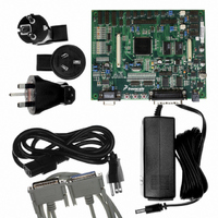
EVAL BOARD FOR MC56F83X
Manufacturer
Freescale Semiconductor
Type
DSPr
Specifications of MC56F8367EVME
Contents
Module and Misc Hardware
Processor To Be Evaluated
MC56F8145-67 and MC56F8345-67
Data Bus Width
16 bit
Interface Type
RS-232
Silicon Manufacturer
Freescale
Core Architecture
56800/E
Core Sub-architecture
56800/E
Silicon Core Number
MC56F
Silicon Family Name
MC56F83xx
Rohs Compliant
Yes
For Use With/related Products
MC56F83x5, MC56F83x6, MC56F83x7
Lead Free Status / RoHS Status
Lead free / RoHS Compliant


the OCCS_COHL bit high as well.
3.3 Registers
When referring to the register definitions for the OCCS in the 56F8300 Peripheral User Manual, use the
register definitions without the internal Relaxation Oscillator, since the 56F8367/56F8167 do NOT
contain this oscillator.
Part 4 Memory Operating Modes (MEM)
4.1 Introduction
The 56F8367 and 56F8167 devices are 16-bit motor-control chips based on the 56800E core. These parts
use a Harvard-style architecture with two independent memory spaces for Data and Program. On-chip
RAM and Flash memory are used in both spaces.
This chapter provides memory maps for:
On-chip memory sizes for each device are summarized in
identified in the “Use Restrictions” column of
Note: Data Flash and Program RAM are NOT available on the 56F8167 device.
Freescale Semiconductor
Preliminary
Program Flash
Data Flash
Program RAM
Data RAM
Program Boot Flash
•
•
On-Chip Memory
Program Address Space including the Interrupt Vector Table
Data Address Space including the EOnCE Memory and Peripheral Memory Maps
Figure 3-4 Connecting an External Clock Register
External
XTAL
Clock
56F8367
512KB
32KB
32KB
32KB
4KB
Table 4-1 Chip Memory Configurations
EXTAL
V
SS
56F8367 Technical Data, Rev. 8
56F8167
512KB
32KB
32KB
—
—
Note: When using an external clocking source with
this configuration, the input “CLKMODE” should be
high and the COHL bit in the OSCTL register
should be set to 1.
Table
Erase/Program via Flash interface unit and word writes to
CDBW
Erase/Program via Flash interface unit and word writes to
CDBW. Data Flash can be read via one of CDBR or XDB2, but
not both simultaneously
None
None
Erase/Program via Flash Interface unit and word to CDWB
4-1.
Table
4-1. Flash memories’ restrictions are
Use Restrictions
Registers
41
Related parts for MC56F8367EVME
Image
Part Number
Description
Manufacturer
Datasheet
Request
R

Part Number:
Description:
56f8300 16-bit Digital Signal Controllers
Manufacturer:
Freescale Semiconductor, Inc
Datasheet:
Part Number:
Description:
Manufacturer:
Freescale Semiconductor, Inc
Datasheet:
Part Number:
Description:
Manufacturer:
Freescale Semiconductor, Inc
Datasheet:
Part Number:
Description:
Manufacturer:
Freescale Semiconductor, Inc
Datasheet:
Part Number:
Description:
Manufacturer:
Freescale Semiconductor, Inc
Datasheet:
Part Number:
Description:
Manufacturer:
Freescale Semiconductor, Inc
Datasheet:
Part Number:
Description:
Manufacturer:
Freescale Semiconductor, Inc
Datasheet:
Part Number:
Description:
Manufacturer:
Freescale Semiconductor, Inc
Datasheet:
Part Number:
Description:
Manufacturer:
Freescale Semiconductor, Inc
Datasheet:
Part Number:
Description:
Manufacturer:
Freescale Semiconductor, Inc
Datasheet:
Part Number:
Description:
Manufacturer:
Freescale Semiconductor, Inc
Datasheet:
Part Number:
Description:
Manufacturer:
Freescale Semiconductor, Inc
Datasheet:
Part Number:
Description:
Manufacturer:
Freescale Semiconductor, Inc
Datasheet:
Part Number:
Description:
Manufacturer:
Freescale Semiconductor, Inc
Datasheet:
Part Number:
Description:
Manufacturer:
Freescale Semiconductor, Inc
Datasheet: