MC56F8367EVME Freescale Semiconductor, MC56F8367EVME Datasheet - Page 25
MC56F8367EVME
Manufacturer Part Number
MC56F8367EVME
Description
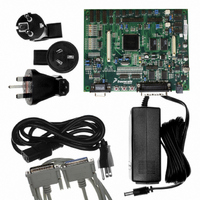
EVAL BOARD FOR MC56F83X
Manufacturer
Freescale Semiconductor
Type
DSPr
Specifications of MC56F8367EVME
Contents
Module and Misc Hardware
Processor To Be Evaluated
MC56F8145-67 and MC56F8345-67
Data Bus Width
16 bit
Interface Type
RS-232
Silicon Manufacturer
Freescale
Core Architecture
56800/E
Core Sub-architecture
56800/E
Silicon Core Number
MC56F
Silicon Family Name
MC56F83xx
Rohs Compliant
Yes
For Use With/related Products
MC56F83x5, MC56F83x6, MC56F83x7
Lead Free Status / RoHS Status
Lead free / RoHS Compliant


Freescale Semiconductor
Preliminary
Table 2-2 Signal and Package Information for the 160-Pin LQFP and MBGA (Continued)
(GPIOD8)
(GPIOD9)
Signal
Name
(CS0)
(CS1)
WR
PS
DS
No.
Pin
51
53
54
Ball No.
N6
L4
L5
Output
Output
Output
Output
Output
Input/
Input/
Type
56F8367 Technical Data, Rev. 8
disabled,
pull-up is
disabled,
pull-up is
disabled,
pull-up is
output is
output is
output is
In reset,
In reset,
In reset,
enabled
enabled
enabled
During
Reset
State
Write Enable — WR is asserted during external memory write
cycles. When WR is asserted low, pins D0 - D15 become outputs
and the device puts data on the bus. When WR is deasserted
high, the external data is latched inside the external device. When
WR is asserted, it qualifies the A0 - A23, PS, DS, and CSn pins.
WR can be connected directly to the WE pin of a static RAM.
Depending upon the state of the DRV bit in the EMI bus control
register (BCR), WR is tri-stated when the external bus is inactive.
Most designs will want to change the DRV state to DRV = 1 instead
of using the default setting.
To deactivate the internal pull-up resistor, set the CTRL bit in the
SIM_PUDR register.
Program Memory Select — This signal is actually CS0 in the
EMI, which is programmed at reset for compatibility with the
56F80x PS signal. PS is asserted low for external program
memory access.
Depending upon the state of the DRV bit in the EMI bus control
register (BCR), CS0 is tri-stated when the external bus is inactive.
CS0 resets to provide the PS function as defined on the 56F80x
devices.
Port D GPIO — This GPIO pin can be individually programmed
as an input or output pin.
To deactivate the internal pull-up resistor, clear bit 8 in the
GPIOD_PUR register.
Data Memory Select — This signal is actually CS1 in the EMI,
which is programmed at reset for compatibility with the 56F80x
DS signal. DS is asserted low for external data memory access.
Depending upon the state of the DRV bit in the EMI bus control
register (BCR), CS1 is tri-stated when the external bus is inactive.
CS1 resets to provide the DS function as defined on the 56F80x
devices.
Port D GPIO — This GPIO pin can be individually programmed
as an input or output pin.
To deactivate the internal pull-up resistor, clear bit 9 in the
GPIOD_PUR register.
Signal Description
Signal Pins
25
Related parts for MC56F8367EVME
Image
Part Number
Description
Manufacturer
Datasheet
Request
R

Part Number:
Description:
56f8300 16-bit Digital Signal Controllers
Manufacturer:
Freescale Semiconductor, Inc
Datasheet:
Part Number:
Description:
Manufacturer:
Freescale Semiconductor, Inc
Datasheet:
Part Number:
Description:
Manufacturer:
Freescale Semiconductor, Inc
Datasheet:
Part Number:
Description:
Manufacturer:
Freescale Semiconductor, Inc
Datasheet:
Part Number:
Description:
Manufacturer:
Freescale Semiconductor, Inc
Datasheet:
Part Number:
Description:
Manufacturer:
Freescale Semiconductor, Inc
Datasheet:
Part Number:
Description:
Manufacturer:
Freescale Semiconductor, Inc
Datasheet:
Part Number:
Description:
Manufacturer:
Freescale Semiconductor, Inc
Datasheet:
Part Number:
Description:
Manufacturer:
Freescale Semiconductor, Inc
Datasheet:
Part Number:
Description:
Manufacturer:
Freescale Semiconductor, Inc
Datasheet:
Part Number:
Description:
Manufacturer:
Freescale Semiconductor, Inc
Datasheet:
Part Number:
Description:
Manufacturer:
Freescale Semiconductor, Inc
Datasheet:
Part Number:
Description:
Manufacturer:
Freescale Semiconductor, Inc
Datasheet:
Part Number:
Description:
Manufacturer:
Freescale Semiconductor, Inc
Datasheet:
Part Number:
Description:
Manufacturer:
Freescale Semiconductor, Inc
Datasheet: