MC56F8367EVME Freescale Semiconductor, MC56F8367EVME Datasheet - Page 117
MC56F8367EVME
Manufacturer Part Number
MC56F8367EVME
Description
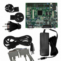
EVAL BOARD FOR MC56F83X
Manufacturer
Freescale Semiconductor
Type
DSPr
Specifications of MC56F8367EVME
Contents
Module and Misc Hardware
Processor To Be Evaluated
MC56F8145-67 and MC56F8345-67
Data Bus Width
16 bit
Interface Type
RS-232
Silicon Manufacturer
Freescale
Core Architecture
56800/E
Core Sub-architecture
56800/E
Silicon Core Number
MC56F
Silicon Family Name
MC56F83xx
Rohs Compliant
Yes
For Use With/related Products
MC56F83x5, MC56F83x6, MC56F83x7
Lead Free Status / RoHS Status
Lead free / RoHS Compliant


6.5.4
This read-only register displays the most significant half of the JTAG ID for the chip. This register reads
$01D6.
6.5.5
This read-only register displays the least significant half of the JTAG ID for the chip. This register reads
$D01D.
6.5.6
Most of the pins on the chip have on-chip pull-up resistors. Pins which can operate as GPIO can have these
resistors disabled via the GPIO function. Non-GPIO pins can have their pull-ups disabled by setting the
appropriate bit in this register. Disabling pull-ups is done on a peripheral-by-peripheral basis (for pins not
muxed with GPIO). Each bit in the register (see
Table 2-2
6.5.6.1
This bit field is reserved or not implemented. It is read as 0 and cannot be modified by writing.
6.5.6.2
This bit controls the pull-up resistors on the FAULTA3 pin.
Freescale Semiconductor
Preliminary
Base + $8
RESET
Write
Read
Base + $6
Base + $7
RESET
RESET
Read
Write
Read
Write
to identify which pins can deactivate the internal pull-up resistor.
Most Significant Half of JTAG ID (SIM_MSH_ID)
Least Significant Half of JTAG ID (SIM_LSH_ID)
SIM Pull-up Disable Register (SIM_PUDR)
Reserved —Bit 15
PWMA1—Bit 14
15
0
0
15
15
PWMA1
Figure 6-6 Most Significant Half of JTAG ID (SIM_MSH_ID)
Figure 6-7 Least Significant Half of JTAG ID (SIM_LSH_ID)
0
0
1
1
14
0
Figure 6-8 SIM Pull-up Disable Register (SIM_PUDR)
14
14
0
0
1
1
CAN
13
0
13
13
0
0
0
0
MODE
EMI_
12
0
12
12
0
0
1
1
RESET
11
0
56F8367 Technical Data, Rev. 8
11
11
0
0
0
0
IRQ
10
0
10
10
0
0
0
0
XBOOT PWMB PWMA0
Figure
9
0
9
0
0
9
0
0
6-8) corresponds to a functional group of pins. See
8
0
8
8
1
1
0
0
7
0
7
7
1
1
0
0
6
6
1
1
0
0
6
0
0
CTRL
5
0
0
5
0
0
5
0
4
1
1
4
1
1
4
0
0
JTAG
3
3
3
0
0
0
1
1
2
1
1
2
1
1
2
0
0
Register Descriptions
1
1
1
1
0
0
1
0
0
0
0
0
0
1
1
0
0
0
117
Related parts for MC56F8367EVME
Image
Part Number
Description
Manufacturer
Datasheet
Request
R

Part Number:
Description:
56f8300 16-bit Digital Signal Controllers
Manufacturer:
Freescale Semiconductor, Inc
Datasheet:
Part Number:
Description:
Manufacturer:
Freescale Semiconductor, Inc
Datasheet:
Part Number:
Description:
Manufacturer:
Freescale Semiconductor, Inc
Datasheet:
Part Number:
Description:
Manufacturer:
Freescale Semiconductor, Inc
Datasheet:
Part Number:
Description:
Manufacturer:
Freescale Semiconductor, Inc
Datasheet:
Part Number:
Description:
Manufacturer:
Freescale Semiconductor, Inc
Datasheet:
Part Number:
Description:
Manufacturer:
Freescale Semiconductor, Inc
Datasheet:
Part Number:
Description:
Manufacturer:
Freescale Semiconductor, Inc
Datasheet:
Part Number:
Description:
Manufacturer:
Freescale Semiconductor, Inc
Datasheet:
Part Number:
Description:
Manufacturer:
Freescale Semiconductor, Inc
Datasheet:
Part Number:
Description:
Manufacturer:
Freescale Semiconductor, Inc
Datasheet:
Part Number:
Description:
Manufacturer:
Freescale Semiconductor, Inc
Datasheet:
Part Number:
Description:
Manufacturer:
Freescale Semiconductor, Inc
Datasheet:
Part Number:
Description:
Manufacturer:
Freescale Semiconductor, Inc
Datasheet:
Part Number:
Description:
Manufacturer:
Freescale Semiconductor, Inc
Datasheet: