MC56F8367EVME Freescale Semiconductor, MC56F8367EVME Datasheet - Page 35
MC56F8367EVME
Manufacturer Part Number
MC56F8367EVME
Description
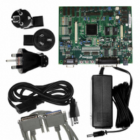
EVAL BOARD FOR MC56F83X
Manufacturer
Freescale Semiconductor
Type
DSPr
Specifications of MC56F8367EVME
Contents
Module and Misc Hardware
Processor To Be Evaluated
MC56F8145-67 and MC56F8345-67
Data Bus Width
16 bit
Interface Type
RS-232
Silicon Manufacturer
Freescale
Core Architecture
56800/E
Core Sub-architecture
56800/E
Silicon Core Number
MC56F
Silicon Family Name
MC56F83xx
Rohs Compliant
Yes
For Use With/related Products
MC56F83x5, MC56F83x6, MC56F83x7
Lead Free Status / RoHS Status
Lead free / RoHS Compliant


Freescale Semiconductor
Preliminary
Table 2-2 Signal and Package Information for the 160-Pin LQFP and MBGA (Continued)
(GPIOD10)
(GPIOD11)
(GPIOD12)
FAULTB0
FAULTB1
FAULTB2
FAULTB3
V
V
Signal
V
V
V
Name
ANA0
ANA1
ANA2
ANA3
ANA4
ANA5
ANA6
ANA7
REFMID
ISB0
ISB1
ISB2
REFLO
REFH
REFP
REFN
No.
100
101
102
103
104
105
106
107
113
112
111
110
109
Pin
61
63
64
67
68
69
72
Ball No.
G13
H13
G12
H14
G14
D14
D13
P11
F13
F12
E13
E14
F14
E12
L10
N8
N9
P8
L8
L9
Schmitt
Schmitt
Schmitt
Output
Output
Input/
Input/
Type
Input
Input
Input
Input
Input
Input
56F8367 Technical Data, Rev. 8
enabled
enabled
During
Analog
Analog
Analog
Analog
Analog
pull-up
pull-up
Output
Reset
State
Input,
Input,
Input/
Input
Input
Input
Input
ISB0 - 2 — These three input current status pins are used for
top/bottom pulse width correction in complementary channel
operation for PWMB.
Port D GPIO — These GPIO pins can be individually
programmed as input or output pins.
At reset, these pins default to ISB functionality.
To deactivate the internal pull-up resistor, clear the appropriate bit
of the GPIOD_PUR register. For details, see
FAULTB0 - 3 — These four fault input pins are used for disabling
selected PWMB outputs in cases where fault conditions originate
off-chip.
To deactivate the internal pull-up resistor, set the PWMB bit in the
SIM_PUDR register. For details, see
ANA0 - 3 — Analog inputs to ADC A, channel 0
ANA4 - 7 — Analog inputs to ADC A, channel 1
V
than or equal to V
V
which are brought off-chip so they can be bypassed. Connect to a
0.1μF low ESR capacitor.
V
be connected to a low-noise V
REFH
REFP
REFLO
, V
— Analog Reference Voltage High. V
— Analog Reference Voltage Low. This should normally
REFMID
& V
DDA_ADC.
REFN
Signal Description
— Internal pins for voltage reference
SS
.
Part
6.5.8.
REFH
Part
must be less
6.5.8.
Signal Pins
35
Related parts for MC56F8367EVME
Image
Part Number
Description
Manufacturer
Datasheet
Request
R

Part Number:
Description:
56f8300 16-bit Digital Signal Controllers
Manufacturer:
Freescale Semiconductor, Inc
Datasheet:
Part Number:
Description:
Manufacturer:
Freescale Semiconductor, Inc
Datasheet:
Part Number:
Description:
Manufacturer:
Freescale Semiconductor, Inc
Datasheet:
Part Number:
Description:
Manufacturer:
Freescale Semiconductor, Inc
Datasheet:
Part Number:
Description:
Manufacturer:
Freescale Semiconductor, Inc
Datasheet:
Part Number:
Description:
Manufacturer:
Freescale Semiconductor, Inc
Datasheet:
Part Number:
Description:
Manufacturer:
Freescale Semiconductor, Inc
Datasheet:
Part Number:
Description:
Manufacturer:
Freescale Semiconductor, Inc
Datasheet:
Part Number:
Description:
Manufacturer:
Freescale Semiconductor, Inc
Datasheet:
Part Number:
Description:
Manufacturer:
Freescale Semiconductor, Inc
Datasheet:
Part Number:
Description:
Manufacturer:
Freescale Semiconductor, Inc
Datasheet:
Part Number:
Description:
Manufacturer:
Freescale Semiconductor, Inc
Datasheet:
Part Number:
Description:
Manufacturer:
Freescale Semiconductor, Inc
Datasheet:
Part Number:
Description:
Manufacturer:
Freescale Semiconductor, Inc
Datasheet:
Part Number:
Description:
Manufacturer:
Freescale Semiconductor, Inc
Datasheet: