MC56F8367EVME Freescale Semiconductor, MC56F8367EVME Datasheet - Page 22
MC56F8367EVME
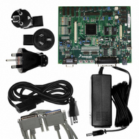
Manufacturer Part Number
MC56F8367EVME
Description
EVAL BOARD FOR MC56F83X
Manufacturer
Freescale Semiconductor
Type
DSPr
Specifications of MC56F8367EVME
Contents
Module and Misc Hardware
Processor To Be Evaluated
MC56F8145-67 and MC56F8345-67
Data Bus Width
16 bit
Interface Type
RS-232
Silicon Manufacturer
Freescale
Core Architecture
56800/E
Core Sub-architecture
56800/E
Silicon Core Number
MC56F
Silicon Family Name
MC56F83xx
Rohs Compliant
Yes
For Use With/related Products
MC56F83x5, MC56F83x6, MC56F83x7
Lead Free Status / RoHS Status
Lead free / RoHS Compliant


22
(SYS_CLK2)
Table 2-2 Signal and Package Information for the 160-Pin LQFP and MBGA (Continued)
(prescaler_
(oscillator_
(SYS_CLK)
GPIOB0
GPIOB1
GPIOB2
GPIOB3
GPIOB4
GPIOB5
GPIOB6
GPIOB7
Signal
clock)
clock)
Name
(A16)
(A17)
(A18)
(A19)
(A20)
(A21)
(A22)
(A23)
No.
Pin
33
34
35
36
37
46
47
48
Ball No.
M1
M2
N4
M4
P3
L1
L3
L2
Schmitt
Schmitt
Output
Output
Output
Output
Output
Input/
Input/
Type
56F8367 Technical Data, Rev. 8
enabled
enabled
During
pull-up
pull-up
Reset
State
Input,
Input,
Port B GPIO — These four GPIO pins can be programmed as
input or output pins.
Address Bus — A16 - A19 specify one of the address lines for
external program or data memory accesses.
Depending upon the state of the DRV bit in the EMI bus control
register (BCR), A16 - A19 and EMI control signals are tri-stated
when the external bus is inactive.
Most designs will want to change the DRV state to DRV = 1 instead
of using the default setting.
After reset, the startup state of GPIOB0 - GPIOB3 (GPIO or
address) is determined as a function of EXTBOOT, EMI_MODE
and the Flash security setting. See
information on when this pin is configured as an address pin at
reset. In all cases, this state may be changed by writing to
GPIOB_PER.
To deactivate the internal pull-up resistor, clear the appropriate
GPIO bit in the GPIOB_PUR register.
Port B GPIO — These four GPIO pins can be programmed as
input or output pins.
Address Bus — A20 - A23 specify one of the address lines for
external program or data memory accesses.
Depending upon the state of the DRV bit in the EMI bus control
register (BCR), A20–A23 and EMI control signals are tri-stated when
the external bus is inactive.
Most designs will want to change the DRV state to DRV = 1 instead
of using the default setting.
Clock Outputs — can be used to monitor the prescaler_clock,
SYS_CLK, SYS_CLK2 or oscillator_clock on GPIOB4 through
GPIOB7, respectively.
After reset, the default state is GPIO.
These pins can also be used to extend the external address bus
to its full length or to view any of several system clocks. In these
cases, the GPIO_B_PER can be used to individually disable the
GPIO. The CLKOSR register in the SIM (see
be used to choose between address and clock functions.
Signal Description
Table 4-4
Freescale Semiconductor
Part
for further
6.5.7) can then
Preliminary
Related parts for MC56F8367EVME
Image
Part Number
Description
Manufacturer
Datasheet
Request
R

Part Number:
Description:
56f8300 16-bit Digital Signal Controllers
Manufacturer:
Freescale Semiconductor, Inc
Datasheet:
Part Number:
Description:
Manufacturer:
Freescale Semiconductor, Inc
Datasheet:
Part Number:
Description:
Manufacturer:
Freescale Semiconductor, Inc
Datasheet:
Part Number:
Description:
Manufacturer:
Freescale Semiconductor, Inc
Datasheet:
Part Number:
Description:
Manufacturer:
Freescale Semiconductor, Inc
Datasheet:
Part Number:
Description:
Manufacturer:
Freescale Semiconductor, Inc
Datasheet:
Part Number:
Description:
Manufacturer:
Freescale Semiconductor, Inc
Datasheet:
Part Number:
Description:
Manufacturer:
Freescale Semiconductor, Inc
Datasheet:
Part Number:
Description:
Manufacturer:
Freescale Semiconductor, Inc
Datasheet:
Part Number:
Description:
Manufacturer:
Freescale Semiconductor, Inc
Datasheet:
Part Number:
Description:
Manufacturer:
Freescale Semiconductor, Inc
Datasheet:
Part Number:
Description:
Manufacturer:
Freescale Semiconductor, Inc
Datasheet:
Part Number:
Description:
Manufacturer:
Freescale Semiconductor, Inc
Datasheet:
Part Number:
Description:
Manufacturer:
Freescale Semiconductor, Inc
Datasheet:
Part Number:
Description:
Manufacturer:
Freescale Semiconductor, Inc
Datasheet: