MC56F8367EVME Freescale Semiconductor, MC56F8367EVME Datasheet - Page 132
MC56F8367EVME
Manufacturer Part Number
MC56F8367EVME
Description
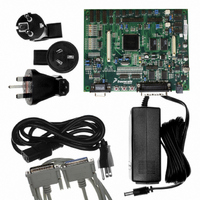
EVAL BOARD FOR MC56F83X
Manufacturer
Freescale Semiconductor
Type
DSPr
Specifications of MC56F8367EVME
Contents
Module and Misc Hardware
Processor To Be Evaluated
MC56F8145-67 and MC56F8345-67
Data Bus Width
16 bit
Interface Type
RS-232
Silicon Manufacturer
Freescale
Core Architecture
56800/E
Core Sub-architecture
56800/E
Silicon Core Number
MC56F
Silicon Family Name
MC56F83xx
Rohs Compliant
Yes
For Use With/related Products
MC56F83x5, MC56F83x6, MC56F83x7
Lead Free Status / RoHS Status
Lead free / RoHS Compliant


EXAMPLE 2: In this example, the system clock has been set up with a value of 32MHz, making the FM
input clock 16MHz. Because that is greater than 12.8MHz, PRDIV8 = FM_CLKDIV[6] = 1. Using the
following equation yields a DIV value of 9 for a clock of 200kHz, and a DIV value of 10 for a clock of
181kHz. This translates to an FM_CLKDIV[6:0] value of $49 or $4A, respectively.
Once the LOCKOUT_RECOVERY instruction has been shifted into the instruction register, the clock
divider value must be shifted into the corresponding 7-bit data register. After the data register has been
updated, the user must transition the TAP controller into the RUN-TEST/IDLE state for the lockout
sequence to commence. The controller must remain in this state until the erase sequence has completed.
For details, see the JTAG Section in the 56F8300 Peripheral User Manual.
Note:
7.2.4
The recommended method of unsecuring a programmed device for product analysis of field failures is via
the backdoor key access. The customer would need to supply Technical Support with the backdoor key
and the protocol to access the backdoor routine in the Flash. Additionally, the KEYEN bit that allows
backdoor key access must be set.
An alternative method for performing analysis on a secured microcontroller would be to mass-erase and
reprogram the Flash with the original code, but modify the security bytes.
To insure that a customer does not inadvertently lock himself out of the device during programming, it is
recommended that he program the backdoor access key first, his application code second, and the security
bytes within the FM configuration field last.
Part 8 General Purpose Input/Output (GPIO)
8.1 Introduction
This section is intended to supplement the GPIO information found in the 56F8300 Peripheral User
Manual and contains only chip-specific information. This information supercedes the generic information
in the 56F8300 Peripheral User Manual.
8.2 Memory Maps
The width of the GPIO port defines how many bits are implemented in each of the GPIO registers. Based
on this and the default function of each of the GPIO pins, the reset values of the GPIOx_PUR and
GPIOx_PER registers will change from port to port.
registers.
132
Once the lockout recovery sequence has completed, the user must reset both the JTAG TAP controller
(by asserting TRST) and the
operation.
Product Analysis
150[kHz]
device
56F8367 Technical Data, Rev. 8
<
(by asserting external chip reset) to return to normal unsecured
(
SYS_CLK
(DIV + 1)
(2)(8)
Table 8-3
)
<
200[kHz]
defines the actual reset values of these
Freescale Semiconductor
Preliminary
Related parts for MC56F8367EVME
Image
Part Number
Description
Manufacturer
Datasheet
Request
R

Part Number:
Description:
56f8300 16-bit Digital Signal Controllers
Manufacturer:
Freescale Semiconductor, Inc
Datasheet:
Part Number:
Description:
Manufacturer:
Freescale Semiconductor, Inc
Datasheet:
Part Number:
Description:
Manufacturer:
Freescale Semiconductor, Inc
Datasheet:
Part Number:
Description:
Manufacturer:
Freescale Semiconductor, Inc
Datasheet:
Part Number:
Description:
Manufacturer:
Freescale Semiconductor, Inc
Datasheet:
Part Number:
Description:
Manufacturer:
Freescale Semiconductor, Inc
Datasheet:
Part Number:
Description:
Manufacturer:
Freescale Semiconductor, Inc
Datasheet:
Part Number:
Description:
Manufacturer:
Freescale Semiconductor, Inc
Datasheet:
Part Number:
Description:
Manufacturer:
Freescale Semiconductor, Inc
Datasheet:
Part Number:
Description:
Manufacturer:
Freescale Semiconductor, Inc
Datasheet:
Part Number:
Description:
Manufacturer:
Freescale Semiconductor, Inc
Datasheet:
Part Number:
Description:
Manufacturer:
Freescale Semiconductor, Inc
Datasheet:
Part Number:
Description:
Manufacturer:
Freescale Semiconductor, Inc
Datasheet:
Part Number:
Description:
Manufacturer:
Freescale Semiconductor, Inc
Datasheet:
Part Number:
Description:
Manufacturer:
Freescale Semiconductor, Inc
Datasheet: