MC56F8367EVME Freescale Semiconductor, MC56F8367EVME Datasheet - Page 29
MC56F8367EVME
Manufacturer Part Number
MC56F8367EVME
Description
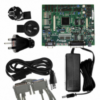
EVAL BOARD FOR MC56F83X
Manufacturer
Freescale Semiconductor
Type
DSPr
Specifications of MC56F8367EVME
Contents
Module and Misc Hardware
Processor To Be Evaluated
MC56F8145-67 and MC56F8345-67
Data Bus Width
16 bit
Interface Type
RS-232
Silicon Manufacturer
Freescale
Core Architecture
56800/E
Core Sub-architecture
56800/E
Silicon Core Number
MC56F
Silicon Family Name
MC56F83xx
Rohs Compliant
Yes
For Use With/related Products
MC56F83x5, MC56F83x6, MC56F83x7
Lead Free Status / RoHS Status
Lead free / RoHS Compliant


Freescale Semiconductor
Preliminary
Table 2-2 Signal and Package Information for the 160-Pin LQFP and MBGA (Continued)
PHASEA0
PHASEB0
(GPIOC4)
(GPIOC5)
Signal
Name
TRST
(TA0)
(TA1)
No.
136
155
156
Pin
Ball No.
D9
A2
B4
Schmitt
Schmitt
Schmitt
Schmitt
Schmitt
Schmitt
Schmitt
Output
Output
Output
Output
Input/
Input/
Input/
Input/
Type
Input
Input
Input
56F8367 Technical Data, Rev. 8
pulled high
internally
enabled
enabled
During
pull-up
pull-up
Reset
State
Input,
Input,
Input,
Test Reset — As an input, a low signal on this pin provides a
reset signal to the JTAG TAP controller. To ensure complete
hardware reset, TRST should be asserted whenever RESET is
asserted. The only exception occurs in a debugging environment
when a hardware device reset is required and the JTAG/EOnCE
module must not be reset. In this case, assert RESET, but do not
assert TRST.
To deactivate the internal pull-up resistor, set the JTAG bit in the
SIM_PUDR register.
Note:
design is to be used in a debugging environment, TRST may be tied to
V
Phase A — Quadrature Decoder 0, PHASEA input
TA0 — Timer A, Channel 0
Port C GPIO — This GPIO pin can be individually programmed
as an input or output pin.
After reset, the default state is PHASEA0.
To deactivate the internal pull-up resistor, clear bit 4 of the
GPIOC_PUR register.
Phase B — Quadrature Decoder 0, PHASEB input
TA1 — Timer A, Channel
Port C GPIO — This GPIO pin can be individually programmed
as an input or output pin.
After reset, the default state is PHASEB0.
To deactivate the internal pull-up resistor, clear bit 5 of the
GPIOC_PUR register.
SS
through a 1K resistor.
For normal operation, connect TRST directly to V
Signal Description
SS
. If the
Signal Pins
29
Related parts for MC56F8367EVME
Image
Part Number
Description
Manufacturer
Datasheet
Request
R

Part Number:
Description:
56f8300 16-bit Digital Signal Controllers
Manufacturer:
Freescale Semiconductor, Inc
Datasheet:
Part Number:
Description:
Manufacturer:
Freescale Semiconductor, Inc
Datasheet:
Part Number:
Description:
Manufacturer:
Freescale Semiconductor, Inc
Datasheet:
Part Number:
Description:
Manufacturer:
Freescale Semiconductor, Inc
Datasheet:
Part Number:
Description:
Manufacturer:
Freescale Semiconductor, Inc
Datasheet:
Part Number:
Description:
Manufacturer:
Freescale Semiconductor, Inc
Datasheet:
Part Number:
Description:
Manufacturer:
Freescale Semiconductor, Inc
Datasheet:
Part Number:
Description:
Manufacturer:
Freescale Semiconductor, Inc
Datasheet:
Part Number:
Description:
Manufacturer:
Freescale Semiconductor, Inc
Datasheet:
Part Number:
Description:
Manufacturer:
Freescale Semiconductor, Inc
Datasheet:
Part Number:
Description:
Manufacturer:
Freescale Semiconductor, Inc
Datasheet:
Part Number:
Description:
Manufacturer:
Freescale Semiconductor, Inc
Datasheet:
Part Number:
Description:
Manufacturer:
Freescale Semiconductor, Inc
Datasheet:
Part Number:
Description:
Manufacturer:
Freescale Semiconductor, Inc
Datasheet:
Part Number:
Description:
Manufacturer:
Freescale Semiconductor, Inc
Datasheet: