MC56F8367EVME Freescale Semiconductor, MC56F8367EVME Datasheet - Page 164
MC56F8367EVME
Manufacturer Part Number
MC56F8367EVME
Description
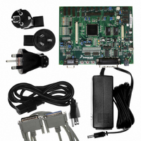
EVAL BOARD FOR MC56F83X
Manufacturer
Freescale Semiconductor
Type
DSPr
Specifications of MC56F8367EVME
Contents
Module and Misc Hardware
Processor To Be Evaluated
MC56F8145-67 and MC56F8345-67
Data Bus Width
16 bit
Interface Type
RS-232
Silicon Manufacturer
Freescale
Core Architecture
56800/E
Core Sub-architecture
56800/E
Silicon Core Number
MC56F
Silicon Family Name
MC56F83xx
Rohs Compliant
Yes
For Use With/related Products
MC56F83x5, MC56F83x6, MC56F83x7
Lead Free Status / RoHS Status
Lead free / RoHS Compliant


10.17 Equivalent Circuit for ADC Inputs
Figure 10-23
at the same time that S3 is closed/open. When S1/S2 are closed & S3 is open, one input of the sample and
hold circuit moves to V
switches are flipped, the charge on C1 and C2 are averaged via S3, with the result that a single-ended
analog input is switched to a differential voltage centered about V
on every cycle of the ADC clock (open one-half ADC clock, closed one-half ADC clock). Note that there
are additional capacitances associated with the analog input pad, routing, etc., but these do not filter into
the S/H output voltage, as S1 provides isolation during the charge-sharing phase.
One aspect of this circuit is that there is an on-going input current, which is a function of the analog input
voltage, V
10.18 Power Consumption
This section provides additional detail which can be used to optimize power consumption for a given
application.
Power consumption is given by the following equation:
A, the internal [static component], is comprised of the DC bias currents for the oscillator, leakage current,
PLL, and voltage references. These sources operate independently of processor state or operating
frequency.
B, the internal [state-dependent component], reflects the supply current required by certain on-chip
resources only when those resources are in use. These include RAM, Flash memory and the ADCs.
164
Total power =
1.
2.
3.
4.
Parasitic capacitance due to package, pin-to-pin and pin-to-package base coupling; 1.8pf
Parasitic capacitance due to the chip bond pad, ESD protection devices and signal routing; 2.04pf
Equivalent resistance for the ESD isolation resistor and the channel select mux; 500 ohms
Sampling capacitor at the sample and hold circuit. Capacitor C1 is normally disconnected from the input and is only
connected to it at sampling time; 1pf
REF
illustrates the ADC input circuit during sample & hold. S1 and S2 are always open/closed
Analog Input
and the ADC clock frequency.
+D: external [dynamic component]
+B: internal [state-dependent component]
+C: internal [dynamic component]
+E: external [static]
A: internal [static component]
1
REFH
Figure 10-23 Equivalent Circuit for A/D Loading
- V
REFH
2
/ 2, while the other charges to the analog input voltage. When the
56F8367 Technical Data, Rev. 8
V
REFH
3
- V
REFH
/ 2
S1
S2
4
S3
REFH
C1
C2
S/H
- V
REFH
C1 = C2 = 1pF
/ 2. The switches switch
Freescale Semiconductor
Preliminary
Related parts for MC56F8367EVME
Image
Part Number
Description
Manufacturer
Datasheet
Request
R

Part Number:
Description:
56f8300 16-bit Digital Signal Controllers
Manufacturer:
Freescale Semiconductor, Inc
Datasheet:
Part Number:
Description:
Manufacturer:
Freescale Semiconductor, Inc
Datasheet:
Part Number:
Description:
Manufacturer:
Freescale Semiconductor, Inc
Datasheet:
Part Number:
Description:
Manufacturer:
Freescale Semiconductor, Inc
Datasheet:
Part Number:
Description:
Manufacturer:
Freescale Semiconductor, Inc
Datasheet:
Part Number:
Description:
Manufacturer:
Freescale Semiconductor, Inc
Datasheet:
Part Number:
Description:
Manufacturer:
Freescale Semiconductor, Inc
Datasheet:
Part Number:
Description:
Manufacturer:
Freescale Semiconductor, Inc
Datasheet:
Part Number:
Description:
Manufacturer:
Freescale Semiconductor, Inc
Datasheet:
Part Number:
Description:
Manufacturer:
Freescale Semiconductor, Inc
Datasheet:
Part Number:
Description:
Manufacturer:
Freescale Semiconductor, Inc
Datasheet:
Part Number:
Description:
Manufacturer:
Freescale Semiconductor, Inc
Datasheet:
Part Number:
Description:
Manufacturer:
Freescale Semiconductor, Inc
Datasheet:
Part Number:
Description:
Manufacturer:
Freescale Semiconductor, Inc
Datasheet:
Part Number:
Description:
Manufacturer:
Freescale Semiconductor, Inc
Datasheet: