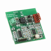
MCP1631RD-DCPC1 Microchip Technology, MCP1631RD-DCPC1 Datasheet - Page 73

MCP1631RD-DCPC1
Manufacturer Part Number
MCP1631RD-DCPC1
Description
REF DES BATT CHARG OR LED DRIVER
Manufacturer
Microchip Technology
Datasheets
1.PIC16F616T-ISL.pdf
(214 pages)
2.MCP1631VHVT-330EST.pdf
(34 pages)
3.MCP1631VHVT-330EST.pdf
(32 pages)
Specifications of MCP1631RD-DCPC1
Current - Output / Channel
700mA
Outputs And Type
1, Non-Isolated
Features
Firmware for Li-Ion, NiMH, and NiCd Battery Charger
Voltage - Input
3.5 ~ 16 V
Utilized Ic / Part
MCP1631HV, PIC16F616
Core Chip
MCP1631HV, PIC16F616
Topology
Parallel, Series
Output Current
1A
No. Of Outputs
1
Input Voltage
3.5V To 16V
Dimming Control Type
Analog
Kit Contents
Board
Lead Free Status / RoHS Status
Lead free / RoHS Compliant
Voltage - Output
-
Lead Free Status / Rohs Status
Lead free / RoHS Compliant
- PIC16F616T-ISL PDF datasheet
- MCP1631VHVT-330EST PDF datasheet #2
- MCP1631VHVT-330EST PDF datasheet #3
- Current page: 73 of 214
- Download datasheet (4Mb)
9.0
The
conversion of an analog input signal to a 10-bit binary
representation of that signal. This device uses analog
inputs, which are multiplexed into a single sample and
hold circuit. The output of the sample and hold is
connected to the input of the converter. The converter
generates a 10-bit binary result via successive
approximation and stores the conversion result into the
ADC result registers (ADRESL and ADRESH).
The ADC voltage reference is software selectable to
either V
pins.
The ADC can generate an interrupt upon completion of
a conversion. This interrupt can be used to wake-up the
device from Sleep.
Figure 9-1 shows the block diagram of the ADC.
FIGURE 9-1:
© 2009 Microchip Technology Inc.
Analog-to-Digital
DD
ANALOG-TO-DIGITAL
CONVERTER (ADC) MODULE
(PIC16F616/16HV616 ONLY)
or a voltage applied to the external reference
0.6V Reference
1.2V Reference
RA1/AN1/V
ADC BLOCK DIAGRAM
RC0/AN4
RC1/AN5
RC2/AN6
RC3/AN7
RA0/AN0
RA2/AN2
RA4/AN3
Converter
CV
REF
REF
CHS <3:0>
(ADC)
V
REF
PIC16F610/616/16HV610/616
allows
4
V
DD
GO/DONE
VCFG = 0
VCFG = 1
ADON
V
SS
Note:
ADC
The ADRESL and ADRESH registers are
read-only.
ADFM
ADRESH ADRESL
0 = Left Justify
1 = Right Justify
10
10
DS41288F-page 73
Related parts for MCP1631RD-DCPC1
Image
Part Number
Description
Manufacturer
Datasheet
Request
R

Part Number:
Description:
REFERENCE DESIGN MCP1631HV
Manufacturer:
Microchip Technology
Datasheet:

Part Number:
Description:
REFERENCE DESIGN FOR MCP1631HV
Manufacturer:
Microchip Technology
Datasheet:

Part Number:
Description:
Manufacturer:
Microchip Technology Inc.
Datasheet:

Part Number:
Description:
Manufacturer:
Microchip Technology Inc.
Datasheet:

Part Number:
Description:
Manufacturer:
Microchip Technology Inc.
Datasheet:

Part Number:
Description:
Manufacturer:
Microchip Technology Inc.
Datasheet:

Part Number:
Description:
Manufacturer:
Microchip Technology Inc.
Datasheet:

Part Number:
Description:
Manufacturer:
Microchip Technology Inc.
Datasheet:

Part Number:
Description:
Manufacturer:
Microchip Technology Inc.
Datasheet:

Part Number:
Description:
Manufacturer:
Microchip Technology Inc.
Datasheet:


