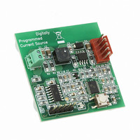
MCP1631RD-DCPC1 Microchip Technology, MCP1631RD-DCPC1 Datasheet - Page 110

MCP1631RD-DCPC1
Manufacturer Part Number
MCP1631RD-DCPC1
Description
REF DES BATT CHARG OR LED DRIVER
Manufacturer
Microchip Technology
Datasheets
1.PIC16F616T-ISL.pdf
(214 pages)
2.MCP1631VHVT-330EST.pdf
(34 pages)
3.MCP1631VHVT-330EST.pdf
(32 pages)
Specifications of MCP1631RD-DCPC1
Current - Output / Channel
700mA
Outputs And Type
1, Non-Isolated
Features
Firmware for Li-Ion, NiMH, and NiCd Battery Charger
Voltage - Input
3.5 ~ 16 V
Utilized Ic / Part
MCP1631HV, PIC16F616
Core Chip
MCP1631HV, PIC16F616
Topology
Parallel, Series
Output Current
1A
No. Of Outputs
1
Input Voltage
3.5V To 16V
Dimming Control Type
Analog
Kit Contents
Board
Lead Free Status / RoHS Status
Lead free / RoHS Compliant
Voltage - Output
-
Lead Free Status / Rohs Status
Lead free / RoHS Compliant
- PIC16F616T-ISL PDF datasheet
- MCP1631VHVT-330EST PDF datasheet #2
- MCP1631VHVT-330EST PDF datasheet #3
- Current page: 110 of 214
- Download datasheet (4Mb)
PIC16F610/616/16HV610/616
REGISTER 12-1:
DS41288F-page 110
bit 15
bit 7
Legend:
R = Readable bit
-n = Value at POR
bit 15-10
bit 9-8
bit 7
bit 6
bit 5
bit 4
bit 3
bit 2-0
Note 1:
IOSCFS
—
2:
3:
Enabling Brown-out Reset does not automatically enable Power-up Timer.
The entire program memory will be erased when the code protection is turned off.
When MCLR is asserted in INTOSC or RC mode, the internal clock oscillator is disabled.
Unimplemented: Read as ‘1’
BOREN<1:0>: Brown-out Reset Selection bits
11 = BOR enabled
10 = BOR enabled during operation and disabled in Sleep
0x = BOR disabled
IOSCFS: Internal Oscillator Frequency Select bit
1 = 8 MHz
0 = 4 MHz
CP: Code Protection bit
1 = Program memory code protection is disabled
0 = Program memory code protection is enabled
MCLRE: MCLR Pin Function Select bit
1 = MCLR pin function is MCLR
0 = MCLR pin function is digital input, MCLR internally tied to V
PWRTE: Power-up Timer Enable bit
1 = PWRT disabled
0 = PWRT enabled
WDTE: Watchdog Timer Enable bit
1 = WDT enabled
0 = WDT disabled
FOSC<2:0>: Oscillator Selection bits
111 = RC oscillator: CLKOUT function on RA4/OSC2/CLKOUT pin, RC on RA5/OSC1/CLKIN
110 = RCIO oscillator: I/O function on RA4/OSC2/CLKOUT pin, RC on RA5/OSC1/CLKIN
101 = INTOSC oscillator: CLKOUT function on RA4/OSC2/CLKOUT pin, I/O function on
100 = INTOSCIO oscillator: I/O function on RA4/OSC2/CLKOUT pin, I/O function on
011 = EC: I/O function on RA4/OSC2/CLKOUT pin, CLKIN on RA5/OSC1/CLKIN
010 = HS oscillator: High-speed crystal/resonator on RA4/OSC2/CLKOUT and RA5/OSC1/CLKIN
001 = XT oscillator: Crystal/resonator on RA4/OSC2/CLKOUT and RA5/OSC1/CLKIN
000 = LP oscillator: Low-power crystal on RA4/OSC2/CLKOUT and RA5/OSC1/CLKIN
CP
—
CONFIG: CONFIGURATION WORD REGISTER
(2)
RA5/OSC1/CLKIN
RA5/OSC1/CLKIN
W = Writable bit
‘1’ = Bit is set
MCLRE
—
(2)
(3)
PWRTE
—
(3)
P = Programmable’
‘0’ = Bit is cleared
WDTE
(1)
—
FOSC2
DD
—
© 2009 Microchip Technology Inc.
U = Unimplemented bit,
read as ‘0’
x = Bit is unknown
BOREN1
FOSC1
(1)
BOREN0
FOSC0
bit 8
bit 0
(1)
Related parts for MCP1631RD-DCPC1
Image
Part Number
Description
Manufacturer
Datasheet
Request
R

Part Number:
Description:
REFERENCE DESIGN MCP1631HV
Manufacturer:
Microchip Technology
Datasheet:

Part Number:
Description:
REFERENCE DESIGN FOR MCP1631HV
Manufacturer:
Microchip Technology
Datasheet:

Part Number:
Description:
Manufacturer:
Microchip Technology Inc.
Datasheet:

Part Number:
Description:
Manufacturer:
Microchip Technology Inc.
Datasheet:

Part Number:
Description:
Manufacturer:
Microchip Technology Inc.
Datasheet:

Part Number:
Description:
Manufacturer:
Microchip Technology Inc.
Datasheet:

Part Number:
Description:
Manufacturer:
Microchip Technology Inc.
Datasheet:

Part Number:
Description:
Manufacturer:
Microchip Technology Inc.
Datasheet:

Part Number:
Description:
Manufacturer:
Microchip Technology Inc.
Datasheet:

Part Number:
Description:
Manufacturer:
Microchip Technology Inc.
Datasheet:


