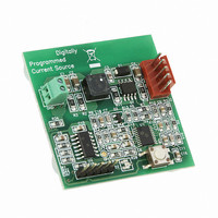
MCP1631RD-DCPC1 Microchip Technology, MCP1631RD-DCPC1 Datasheet - Page 153

MCP1631RD-DCPC1
Manufacturer Part Number
MCP1631RD-DCPC1
Description
REF DES BATT CHARG OR LED DRIVER
Manufacturer
Microchip Technology
Datasheets
1.PIC16F616T-ISL.pdf
(214 pages)
2.MCP1631VHVT-330EST.pdf
(34 pages)
3.MCP1631VHVT-330EST.pdf
(32 pages)
Specifications of MCP1631RD-DCPC1
Current - Output / Channel
700mA
Outputs And Type
1, Non-Isolated
Features
Firmware for Li-Ion, NiMH, and NiCd Battery Charger
Voltage - Input
3.5 ~ 16 V
Utilized Ic / Part
MCP1631HV, PIC16F616
Core Chip
MCP1631HV, PIC16F616
Topology
Parallel, Series
Output Current
1A
No. Of Outputs
1
Input Voltage
3.5V To 16V
Dimming Control Type
Analog
Kit Contents
Board
Lead Free Status / RoHS Status
Lead free / RoHS Compliant
Voltage - Output
-
Lead Free Status / Rohs Status
Lead free / RoHS Compliant
- PIC16F616T-ISL PDF datasheet
- MCP1631VHVT-330EST PDF datasheet #2
- MCP1631VHVT-330EST PDF datasheet #3
- Current page: 153 of 214
- Download datasheet (4Mb)
15.8
© 2009 Microchip Technology Inc.
DC CHARACTERISTICS
D030
D030A
D031
D032
D033
D033A
D040
D040A
D041
D042
D043
D043A
D043B
D060
D061
D063
D070*
D080
D090
Note 1:
Param
No.
2:
3:
4:
5:
*
†
V
V
I
I
V
V
DC Characteristics:
IL
PUR
IL
IH
OL
OH
Sym
These parameters are characterized but not tested.
Data in “Typ” column is at 5.0V, 25°C unless otherwise stated. These parameters are for design guidance only and are
not tested.
In RC oscillator configuration, the OSC1/CLKIN pin is a Schmitt Trigger input. It is not recommended to use an external
clock in RC mode.
Negative current is defined as current sourced by the pin.
The leakage current on the MCLR pin is strongly dependent on the applied voltage level. The specified levels represent
normal operating conditions. Higher leakage current may be measured at different input voltages.
This specification applies to RA3/MCLR configured as RA3 input with internal pull-up disabled.
This specification applies to all weak pull-up pins, including the weak pull-up on RA3/MCLR. When RA3/MCLR is
configured as MCLR reset pin, the weak pull-up is always enabled.
Input Low Voltage
I/O port:
MCLR, OSC1 (RC mode)
OSC1 (XT and LP modes)
OSC1 (HS mode)
Input High Voltage
I/O ports:
MCLR
OSC1 (XT and LP modes)
OSC1 (HS mode)
OSC1 (RC mode)
Input Leakage Current
I/O ports
RA3/MCLR
OSC1
PORTA Weak Pull-up Current
Output Low Voltage
I/O ports
Output High Voltage
I/O ports
with TTL buffer
with TTL buffer
with Schmitt Trigger buffer
with Schmitt Trigger buffer
(2)
Characteristic
(3,4)
PIC16F610/616/16HV610/616
PIC16F610/616/16HV610/616
(2,3)
PIC16F610/616/16HV610/616
(5)
Standard Operating Conditions (unless otherwise stated)
Operating temperature
0.25 V
V
V
0.8 V
0.8 V
0.7 V
0.9 V
DD
DD
Min
Vss
Vss
Vss
V
V
V
2.0
1.6
—
—
—
50
—
—
DD
SS
SS
SS
– 0.7
– 0.7
DD
DD
DD
DD
+ 0.8
Typ†
± 0.1
± 0.7
± 0.1
250
—
—
—
—
—
—
—
—
—
—
—
—
—
—
—
—
—
—
0.15 V
0.2 V
0.2 V
0.3 V
-40°C ≤ T
-40°C ≤ T
Max
V
V
V
V
V
V
V
- I (Industrial)
400
0.8
0.3
0.6
0.6
- E (Extended)
± 1
± 5
± 5
—
—
DD
DD
DD
DD
DD
DD
DD
DD
DD
DD
DD
Units
A
A
μA
μA
μA
μA
≤ +85°C for industrial
≤ +125°C for extended
V
V
V
V
V
V
V
V
V
V
V
V
V
V
V
V
V
4.5V ≤ V
2.0V ≤ V
2.0V ≤ V
4.5V ≤ V
2.0V ≤ V
2.0V ≤ V
(Note 1)
V
Pin at high-impedance
V
V
LP oscillator configuration
V
I
-40°C to +125°C
I
-40°C to +85°C
I
-40°C to +125°C
I
-40°C to +85°C
OL
OL
OH
OH
SS
SS
SS
DD
= 7.0 mA, V
= 8.5 mA, V
= -2.5 mA, V
= -3.0 mA, V
≤ V
≤ V
≤ V
= 5.0V, V
PIN
PIN
PIN
DD
DD
DD
DD
DD
DD
Conditions
DS41288F-page 153
≤ V
≤ V
≤ V
≤ 5.5V
≤ 4.5V
≤ 5.5V
≤ 5.5V
≤ 4.5V
≤ 5.5V
PIN
DD
DD
DD
DD
DD
DD
DD
,
, XT, HS and
= V
= 4.5V,
= 4.5V,
= 4.5V,
= 4.5V,
SS
Related parts for MCP1631RD-DCPC1
Image
Part Number
Description
Manufacturer
Datasheet
Request
R

Part Number:
Description:
REFERENCE DESIGN MCP1631HV
Manufacturer:
Microchip Technology
Datasheet:

Part Number:
Description:
REFERENCE DESIGN FOR MCP1631HV
Manufacturer:
Microchip Technology
Datasheet:

Part Number:
Description:
Manufacturer:
Microchip Technology Inc.
Datasheet:

Part Number:
Description:
Manufacturer:
Microchip Technology Inc.
Datasheet:

Part Number:
Description:
Manufacturer:
Microchip Technology Inc.
Datasheet:

Part Number:
Description:
Manufacturer:
Microchip Technology Inc.
Datasheet:

Part Number:
Description:
Manufacturer:
Microchip Technology Inc.
Datasheet:

Part Number:
Description:
Manufacturer:
Microchip Technology Inc.
Datasheet:

Part Number:
Description:
Manufacturer:
Microchip Technology Inc.
Datasheet:

Part Number:
Description:
Manufacturer:
Microchip Technology Inc.
Datasheet:


