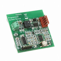
MCP1631RD-DCPC1 Microchip Technology, MCP1631RD-DCPC1 Datasheet - Page 165

MCP1631RD-DCPC1
Manufacturer Part Number
MCP1631RD-DCPC1
Description
REF DES BATT CHARG OR LED DRIVER
Manufacturer
Microchip Technology
Datasheets
1.PIC16F616T-ISL.pdf
(214 pages)
2.MCP1631VHVT-330EST.pdf
(34 pages)
3.MCP1631VHVT-330EST.pdf
(32 pages)
Specifications of MCP1631RD-DCPC1
Current - Output / Channel
700mA
Outputs And Type
1, Non-Isolated
Features
Firmware for Li-Ion, NiMH, and NiCd Battery Charger
Voltage - Input
3.5 ~ 16 V
Utilized Ic / Part
MCP1631HV, PIC16F616
Core Chip
MCP1631HV, PIC16F616
Topology
Parallel, Series
Output Current
1A
No. Of Outputs
1
Input Voltage
3.5V To 16V
Dimming Control Type
Analog
Kit Contents
Board
Lead Free Status / RoHS Status
Lead free / RoHS Compliant
Voltage - Output
-
Lead Free Status / Rohs Status
Lead free / RoHS Compliant
- PIC16F616T-ISL PDF datasheet
- MCP1631VHVT-330EST PDF datasheet #2
- MCP1631VHVT-330EST PDF datasheet #3
- Current page: 165 of 214
- Download datasheet (4Mb)
TABLE 15-10: SHUNT REGULATOR SPECIFICATIONS (PIC16HV610/616 only)
TABLE 15-11: PIC16F616/16HV616 A/D CONVERTER (ADC) CHARACTERISTICS:
© 2009 Microchip Technology Inc.
Standard Operating Conditions (unless otherwise stated)
Operating temperature
AD01
AD02
AD03
AD04
AD07
AD06
AD06A
AD07
AD08
AD09* I
Note 1:
SHUNT REGULATOR CHARACTERISTICS
SR01
SR02
SR03*
SR04
SR05
Param
Param
No.
No.
2:
3:
4:
5:
*
† Data in “Typ” column is at 5.0V, 25°C unless otherwise stated. These parameters are for design guidance
*
N
E
E
E
E
V
V
Z
REF
Sym
REF
AIN
AIN
V
I
T
C
ΔI
IL
DL
OFF
GN
Symbol
R
SHUNT
These parameters are characterized but not tested.
only and are not tested.
Total Absolute Error includes integral, differential, offset and gain errors.
The A/D conversion result never decreases with an increase in the input voltage and has no missing
codes.
ADC V
When ADC is off, it will not consume any current other than leakage current. The power-down current
specification includes any such leakage from the ADC module.
V
These parameters are characterized but not tested.
SETTLE
SHUNT
LOAD
SNT
REF
Resolution
Integral Error
Differential Error
Offset Error
Gain Error
Reference Voltage
Full-Scale Range
Recommended
Impedance of Analog
Voltage Source
V
= 5V for PIC16HV616.
REF
REF
Shunt Voltage
Shunt Current
Settling Time
Load Capacitance
Regulator operating current
Characteristic
Input Current
is from external V
-40°C ≤ T
Characteristics
(3)
(3)
A
≤ +125°C
REF
Min
V
PIC16F610/616/16HV610/616
2.2
2.5
10
—
—
—
—
—
—
—
or V
SS
DD
pin, whichever is selected as reference input.
Typ†
+1.5
Standard Operating Conditions (unless otherwise stated)
Operating temperature
—
—
—
—
—
—
—
—
—
4.75
0.01
Min
—
—
4
10 bits
+ 2.0
V
1000
Max
V
±1
±1
±1
10
50
—
REF
Typ
180
DD
—
—
—
5
Units
LSb V
LSb No missing codes to 10 bits
LSb V
LSb V
kΩ
μA
μA
bit
V
V
Max
150
5.4
50
10
—
V
Absolute minimum to ensure 1 LSb
accuracy
During V
Based on differential of V
During A/D conversion cycle.
REF
REF
REF
REF
-40°C ≤ T
Units
= 5.12V
= 5.12V
= 5.12V
= 5.12V
mA
μF
μA
ns
V
AIN
A
acquisition.
To 1% of final value
Bypass capacitor on V
pin
Includes band gap
reference current
≤ +125°C
Conditions
(5)
(5)
(5)
(5)
Comments
DS41288F-page 165
HOLD
to V
AIN
DD
.
Related parts for MCP1631RD-DCPC1
Image
Part Number
Description
Manufacturer
Datasheet
Request
R

Part Number:
Description:
REFERENCE DESIGN MCP1631HV
Manufacturer:
Microchip Technology
Datasheet:

Part Number:
Description:
REFERENCE DESIGN FOR MCP1631HV
Manufacturer:
Microchip Technology
Datasheet:

Part Number:
Description:
Manufacturer:
Microchip Technology Inc.
Datasheet:

Part Number:
Description:
Manufacturer:
Microchip Technology Inc.
Datasheet:

Part Number:
Description:
Manufacturer:
Microchip Technology Inc.
Datasheet:

Part Number:
Description:
Manufacturer:
Microchip Technology Inc.
Datasheet:

Part Number:
Description:
Manufacturer:
Microchip Technology Inc.
Datasheet:

Part Number:
Description:
Manufacturer:
Microchip Technology Inc.
Datasheet:

Part Number:
Description:
Manufacturer:
Microchip Technology Inc.
Datasheet:

Part Number:
Description:
Manufacturer:
Microchip Technology Inc.
Datasheet:


